Preparation method for silicon nano material and application
A silicon nanotechnology, reaction technology, applied in nanotechnology, nanotechnology, chemical instruments and methods, etc., can solve the problems of high energy consumption and high temperature
- Summary
- Abstract
- Description
- Claims
- Application Information
AI Technical Summary
Problems solved by technology
Method used
Image
Examples
preparation example Construction
[0037] The invention provides a preparation method of silicon nanometer material, comprising: mixing silicon source, reducing agent and molten salt, heating and reacting under airtight conditions to obtain silicon nanometer material; the reducing agent is metal.
[0038] Among them, the present invention has no special limitation on the raw materials for the reaction, which can be commercially available.
[0039] The silicon source can be a silicon-containing material well known to those skilled in the art without any special limitation. In the present invention, it is preferably one or more of silicon-oxygen compounds, silicates, silicon-containing minerals, and biomass; The silicon oxide compound is preferably one or more of silicon dioxide, white carbon black and silicon monoxide; the silicate is preferably a molecular sieve; the silicon-containing mineral is preferably diatomaceous earth, potassium feldspar, One or more of albite, quartz sand and sepiolite; the biomass is ...
Embodiment 1
[0051] Mix 0.6g of silicon dioxide, 0.6g of magnesium powder and 5.0g of anhydrous aluminum trichloride evenly, put it into a 20ml stainless steel autoclave, seal it and place it in a resistance crucible furnace, heat it to 200°C for 10h, and then cool it naturally to room temperature; after opening the kettle, the obtained product was washed with water, washed with 1mol / L dilute hydrochloric acid and centrifuged, and the obtained solid was soaked in hydrofluoric acid for a short period of time for 60 seconds, and then further washed with water and centrifuged to dry to obtain silicon nanomaterials with a yield of 60%.
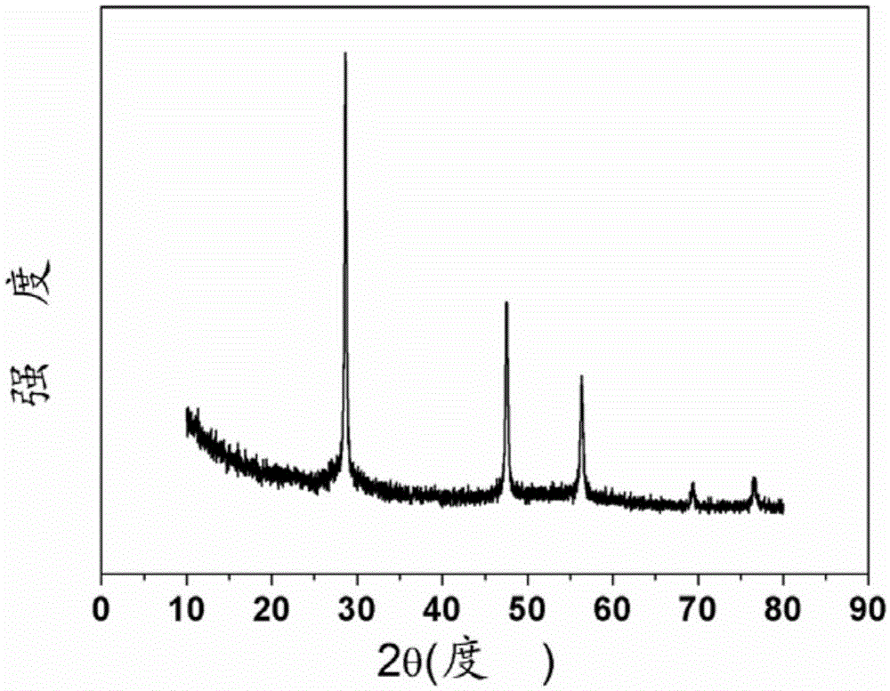
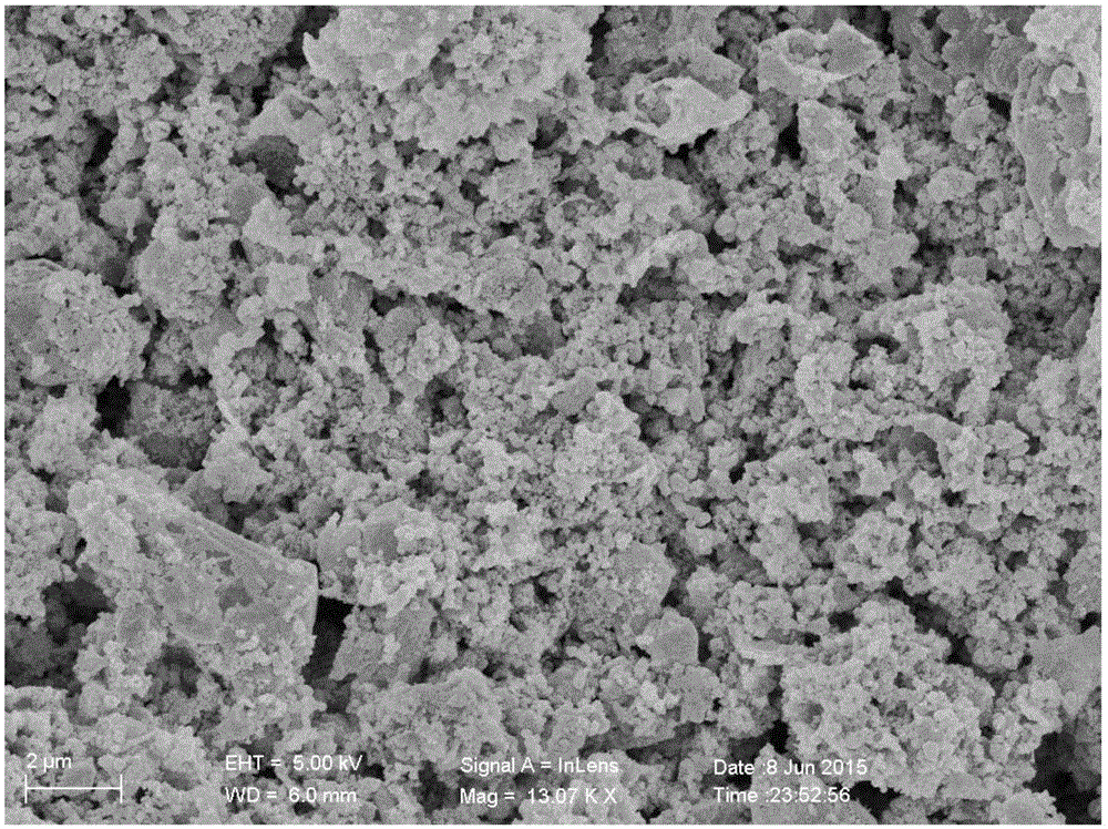
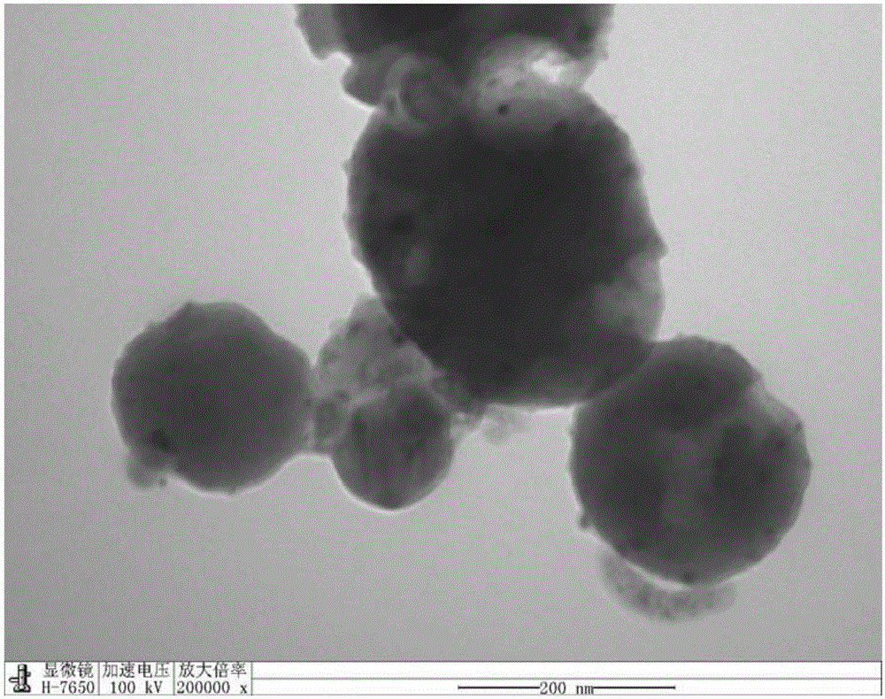
[0052] Utilize X-ray powder diffractometer to carry out X-ray diffraction analysis to the silicon nanomaterial obtained in embodiment 1, obtain its X-ray diffraction spectrum figure such as figure 1 shown. Depend on figure 1 It can be seen that in the X-ray diffraction spectrum, 2θ has clearly visible diffraction peaks in the range of 10° to 80°, and all diff...
Embodiment 2
[0057] Mix 0.6g of silicon dioxide (a by-product of the optical fiber preform of Jiangsu Zhongtian Technology Co., Ltd., with a purity of 99.999%), 0.6g of magnesium powder and 5.0g of anhydrous aluminum trichloride evenly and put them into 20ml of stainless steel high-pressure Kettle, sealed and placed in a resistance crucible furnace, heated to 500 ° C for 10 hours, and then naturally cooled to room temperature; after the kettle was opened, the product obtained was washed with water, washed with 1mol / L dilute hydrochloric acid and centrifuged, and the obtained solid was treated with hydrofluoric acid. Soak for 60 seconds for a short time, then further wash with water and centrifuge and dry to obtain silicon nanomaterials with a yield of 80%.
[0058] Utilize X-ray powder diffractometer to carry out X-ray diffraction analysis to the silicon nanomaterial obtained in embodiment 2, obtain its X-ray diffraction spectrum figure such as Figure 4 shown. Depend on Figure 4 It can...
PUM
 Abstract
Description
Claims
Application Information


