ESD detection method and device and ESD debugging method and device

A detection method and ESD protection technology, applied in the direction of measuring devices, electronic circuit testing, measuring electricity, etc., can solve the problems of low detection efficiency and long time, and achieve the effects of shortening detection time, fast circuit characteristics, and saving detection time

Active Publication Date: 2015-11-25
SEMICON MFG INT (SHANGHAI) CORP +1
View PDF8 Cites 8 Cited by
  • Summary
  • Abstract
  • Description
  • Claims
  • Application Information

AI Technical Summary

Problems solved by technology

There are few disclosures about the existing automatic programming inspection method for the completeness of the on-chip (on-chip) ESD protection circuit on the whole chip, and the inspection is usually only performed at the device level, so it takes a very long time to complete the inspection. Full-chip ESD detection, low detection efficiency

Method used


Image

  • ESD detection method and device and ESD debugging method and device
  • ESD detection method and device and ESD debugging method and device
  • ESD detection method and device and ESD debugging method and device

Examples


Embodiment Construction

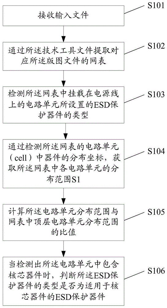
[0045] In the prior art solution, the ESD detection of the chip is usually performed at the device level of the chip. Because the chip contains a lot of devices, the current cutting-edge chip can include more than 1,000,000,000 devices, so it takes a very long time to complete the ESD detection of the whole chip, and the detection efficiency is low. In addition, if the input file is not completely pre-tested before the test is performed, or problems such as program hanged occur during the test, it will further cause unnecessary waste of test time.

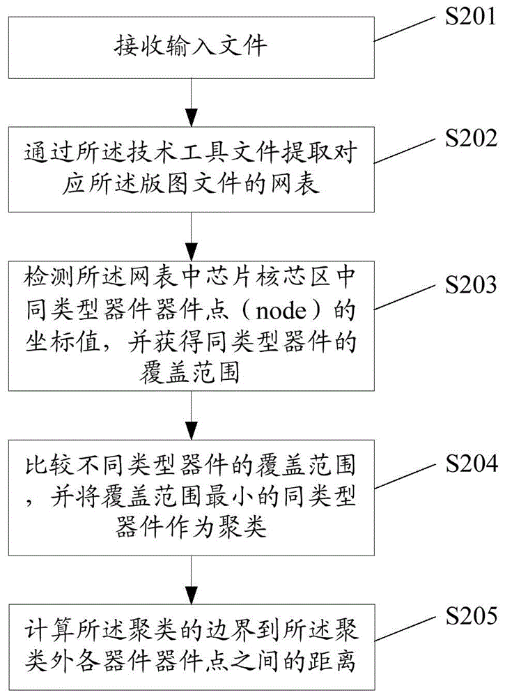
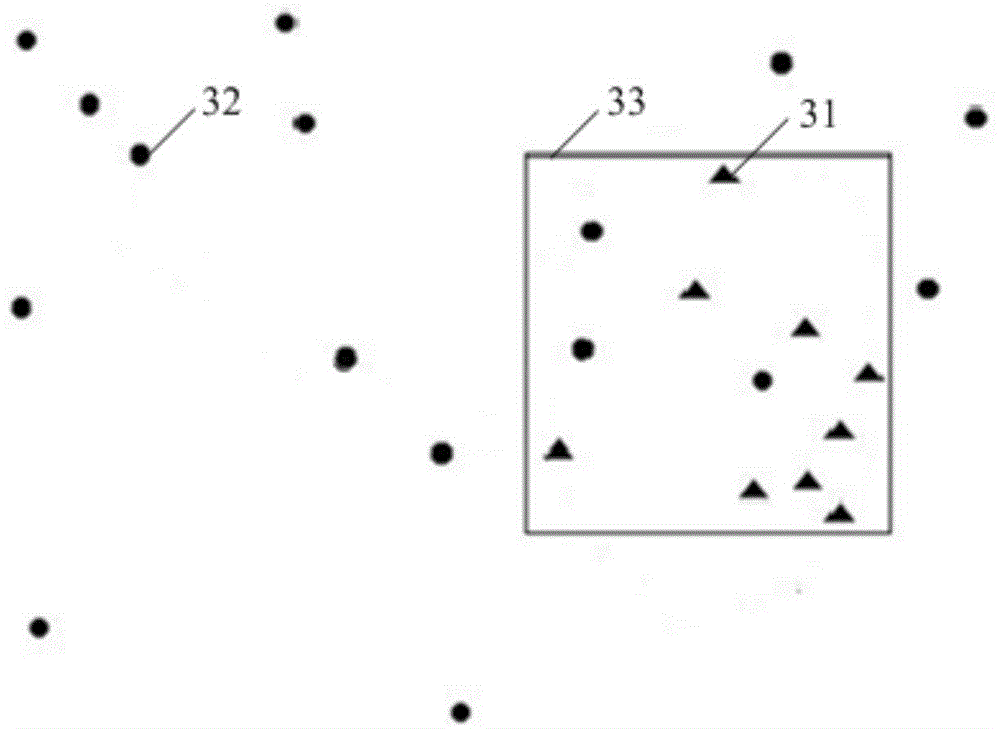
[0046] In the embodiment of the present invention, by detecting the distribution range of each circuit unit in the netlist and the top-level circuit unit, such as the comparison of the area, the detection at the circuit unit level is used instead of the detection at the device level, and it is possible to quickly determine whether the currently loaded circuit unit is Including core devices, the detection time can be reduced exponen...


PUM


Abstract

The invention provides an ESD detection method and device and an ESD debugging method and device. The ESD detection method comprises the steps that an input file is received; a netlist of a corresponding layout file is extracted via a technical tool file; the types of ESD protection devices arranged in circuit units mounted on a power line in the netlist are detected; distribution range of all the circuit units in the netlist is acquired by detecting the distribution coordinates of the devices in the circuit units of the netlist; the specific value of distribution range of all the circuit units to distribution range of top layer circuit units in the netlist is calculated; when the specific value is greater than or equal to a first preset value, the circuit units are judged to include corer devices, and whether the types of the ESD protection devices are the ESD protection devices suitable for the core devices is judged; when the types of the ESD protection devices are the ESD protection devices unsuitable for the core device, the circuit is judged to violate the ESD design rules; and when the specific value is less than the first preset value, whether the circuit units include the core devices is detected. Detection time is reduced by the method and the device.

Description

technical field [0001] The invention relates to electronic equipment detection technology, in particular to an ESD detection method and device, and an ESD debugging method and device. Background technique [0002] Chips are affected by Electro-Static Discharge (ESD) during the entire manufacturing process. When the external environment of the chip or the static charge accumulated inside the chip flows into or out of the chip through the chip pins, a peak current or voltage will be generated in a very short time, causing serious damage to the chip, such as temporary loss of function or permanent damage . In addition, ESD may also absorb dust, shorten the life of the chip, or generate electromagnetic interference, affecting the normal operation of the chip. Therefore, the ESD detection of chips has become an important task in the process of chip development. [0003] There are many components of a chip. At present, a cutting-edge chip may include more than 1,000,000,000 dev...

Claims


Application Information

Patent Timeline
Patent Type & Authority Applications(China)
IPC IPC(8): G01R31/00G01R31/28
Inventor 林松李宏伟
Owner SEMICON MFG INT (SHANGHAI) CORP
Why Eureka
Try Eureka