Supercharge Your Innovation With Domain-Expert AI Agents!

Repair method of low temperature polysilicon array substrate

A technology of low-temperature polysilicon and array substrates, applied in optics, instruments, electrical components, etc., can solve problems such as low yield rate, difficult operation, complicated manufacturing process, etc., and achieve the effect of improving the success rate of repair, improving the yield rate, and easy operation

Active Publication Date: 2018-06-01
WUHAN CHINA STAR OPTOELECTRONICS TECH CO LTD
View PDF6 Cites 1 Cited by
  • Summary
  • Abstract
  • Description
  • Claims
  • Application Information

AI Technical Summary

Problems solved by technology

[0004] However, the manufacturing process of LTPS liquid crystal display panels, especially LTPS array substrates, is relatively complicated, and the yield rate is relatively low. Among them, light leakage and bright spot defects are more common in LTPS liquid crystal display panels
[0005] In the prior art, there are two main ways to repair light leakage and bright spot defects in LTPS liquid crystal display panels: the first way is to interrupt or weld the metal lines corresponding to the defect areas in the array substrate, but the first way is not easy to operate , the repair success rate is also low; the second method is to carbonize the color resist layer corresponding to the defect area in the color filter substrate, which will easily cause the repair area to be too large and the carbonized black spots to be too obvious, which will affect the LCD panel. display quality

Method used


Image

  • Repair method of low temperature polysilicon array substrate
  • Repair method of low temperature polysilicon array substrate
  • Repair method of low temperature polysilicon array substrate

Examples


Embodiment Construction

[0028] In order to further illustrate the technical means adopted by the present invention and its effects, the following describes in detail in conjunction with preferred embodiments of the present invention and accompanying drawings.

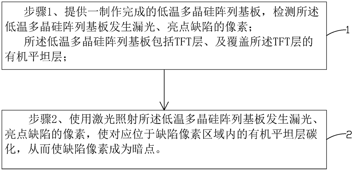
[0029] see figure 1 , the present invention provides a method for repairing a low-temperature polysilicon array substrate, comprising the following steps:

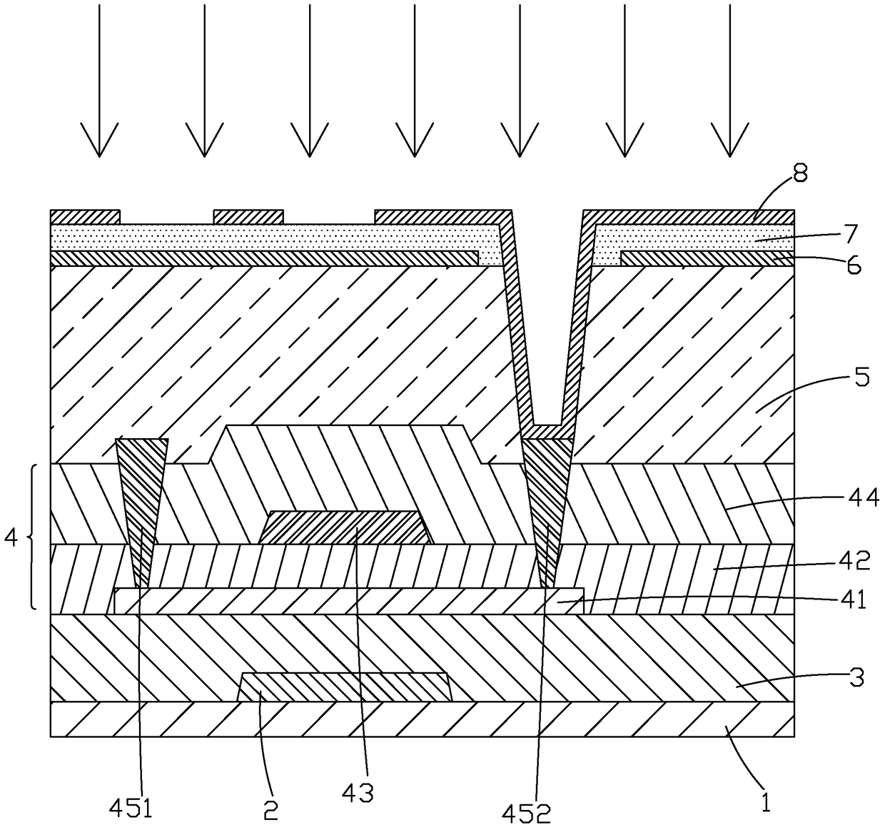
[0030] Step 1. Provide a fabricated low-temperature polysilicon array substrate, and detect pixels with light leakage and bright spot defects on the low-temperature polysilicon array substrate.

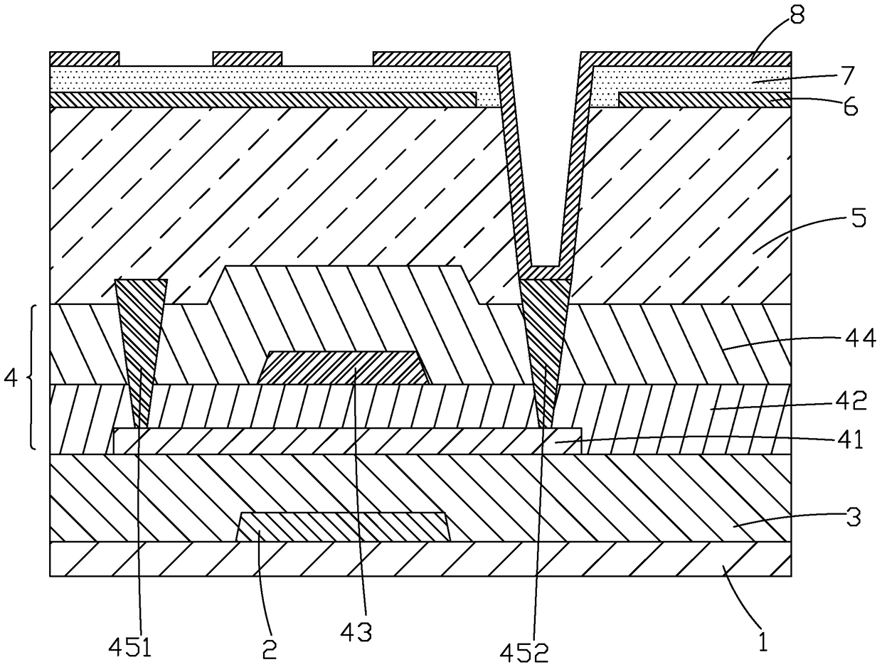
[0031] Specifically, the low temperature polysilicon array substrate may be, but not limited to, an FFS type low temperature polysilicon array substrate. Such as figure 2 As shown, taking an FFS-type low-temperature polysilicon array substrate as an example, the low-temperature polysilicon array substrate includes a glass substrate 1, a light-shielding layer 2 disposed on the glass substrate 1,...


PUM

PropertyMeasurementUnit
wavelengthaaaaaaaaaa

Abstract

The invention provides a repairing method for a low-temperature polycrystalline silicon array substrate. According to the method, laser is used for irradiating the low-temperature polycrystalline silicon array substrate to form pixels with light leakage and light spot defects, and an organic flat layer (5) correspondingly located inside the defect pixel region is carbonized, so that the defect pixels become dark spots, the phenomenon that in the prior art, metal circuits located inside the defect pixel region are broken or fused is avoided, operation is easy and convenient, the light leakage and light spot defects can be effectively repaired, the repairing success rate of the low-temperature polycrystalline silicon liquid crystal display panel is increased, and the yield of the low-temperature polycrystalline silicon liquid crystal display panel is improved.

Description

technical field [0001] The invention relates to the field of display technology, in particular to a method for repairing a low-temperature polysilicon array substrate. Background technique [0002] A liquid crystal display panel is usually composed of a color filter substrate (Color Filter, CF), a thin film transistor array substrate (Thin Film Transistor Array Substrate, TFT Array Substrate), and a liquid crystal layer (Liquid Crystal Layer) arranged between the two substrates. , its working principle is to control the rotation of the liquid crystal molecules in the liquid crystal layer by applying a driving voltage on the two glass substrates, and refract the light from the backlight module to produce a picture. According to the different orientation methods of liquid crystals, the liquid crystal display panels currently on the mainstream market can be divided into the following types: vertical alignment (Vertical Alignment, VA) type, twisted nematic (Twisted Nematic, TN) ...

Claims


Application Information

Patent Timeline
Patent Type & Authority Patents(China)
IPC IPC(8): G02F1/1362H01L27/12
CPCG02F1/136259G02F1/1368H01L27/1259
Inventor 孟林
Owner WUHAN CHINA STAR OPTOELECTRONICS TECH CO LTD
Features
  • R&D
  • Intellectual Property
  • Life Sciences
  • Materials
  • Tech Scout
  • Unparalleled Data Quality
  • Higher Quality Content
  • 60% Fewer Hallucinations
Learn More