Array substrate, preparing method of array substrate, display panel and display device

A technology for an array substrate and a display area, which is applied in the fields of an array substrate and a preparation method thereof, a display panel, and a display device, can solve the problems affecting product quality, signal line breakage, resistance to voltage difference, etc.

Inactive Publication Date: 2015-11-25
BOE TECH GRP CO LTD +1
View PDF4 Cites 16 Cited by
  • Summary
  • Abstract
  • Description
  • Claims
  • Application Information

AI Technical Summary

Problems solved by technology

Because the passivation layer 5 is relatively fragile, at the same time, the signal traces (gate traces 21, common electrode traces 2 or data traces 4) are made of copper with relatively poor compression resistance, and are squeez

Method used


Image

  • Array substrate, preparing method of array substrate, display panel and display device
  • Array substrate, preparing method of array substrate, display panel and display device
  • Array substrate, preparing method of array substrate, display panel and display device

Examples


Example Embodiment

[0054] Example 1:

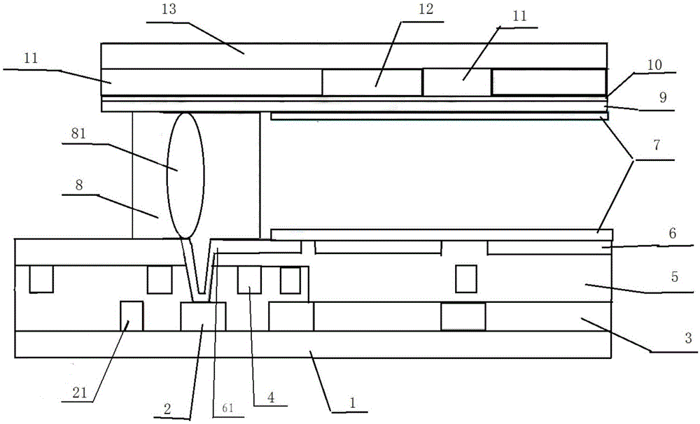
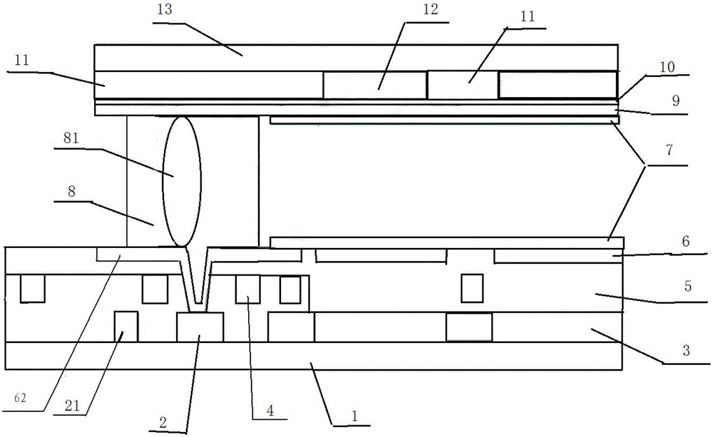
[0055] Such as image 3 As shown, this embodiment provides an array substrate including a display area and a peripheral area. The peripheral area is provided with signal traces. A protection layer 62 is provided in a preset area of ​​the peripheral area. The preset area at least includes Areas with signal routing.

[0056] In the array substrate provided by this embodiment, since a protective layer 62 is provided in the predetermined area of ​​the peripheral area, the protective layer 62 can prevent the gold ball 81 in the frame sealant 8 from moving the signal to the array substrate after being pressed. The line has an adverse effect. That is to say, it can prevent the golden ball 81 from piercing the passivation layer 5, thereby causing a short circuit of the signal wiring.

[0057] Optionally, the protective layer 62 is made of metal or metal oxide. Generally, the hardness of metal or metal oxide is large. At the same time, corresponding to TN type display, ...

Example Embodiment

[0071] Example 2:

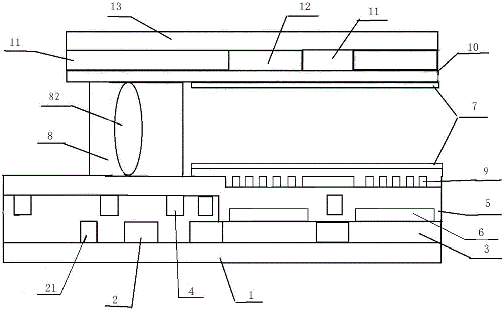
[0072] Such as Figure 4 As shown, this embodiment provides an array substrate including a display area and a peripheral area. The peripheral area is provided with signal traces. A protection layer 62 is provided in a preset area of ​​the peripheral area. The preset area at least includes Areas with signal routing.

[0073] In the array substrate provided in this embodiment, since the protective layer 62 is provided in the predetermined area of ​​the peripheral area, the protective layer 62 can prevent the support such as the silicon balls 82 and / or glass fiber in the frame sealant 8 from being pressed It has an adverse effect on the signal routing of the array substrate. In other words, it can prevent the support such as the silicon ball 82 and / or glass fiber from piercing the passivation layer 5, thereby causing the signal trace to break.

[0074] Optionally, the protective layer 62 is made of metal or metal oxide. Under normal circumstances, metals or metal...

Example Embodiment

[0087] Example 3

[0088] This embodiment provides a method for manufacturing an array substrate, which includes the following steps:

[0089] Forming a thin film transistor on the base substrate;

[0090] The pixel electrode 6 is formed by a patterning process on the base substrate on which the thin film transistor is formed; wherein, the protective layer 62 and the pixel electrode 6 are formed by a single patterning process. The protective layer 62 and the pixel electrode 6 are formed through one patterning process, thereby saving process steps and reducing manufacturing costs.

[0091] Optionally, include the following steps:

[0092] On the base substrate, a gate pattern is formed in the display area of ​​the array substrate through a patterning process, and the gate wiring 21 and the common electrode wiring 2 that are arranged in the same layer as the gate and located in the peripheral area of ​​the array substrate Graphics

[0093] Forming a pattern of the gate insulating layer 3...


PUM


Abstract

The invention provides an array substrate, a preparing method of the array substrate, a display panel and a display device to solve the various poor problems of signal wiring caused by the fact that frame sealing glue in the peripheral area of the array substrate is stressed in the prior art. According to the array substrate, the preparing method of the array substrate, the display panel and the display device, due to the fact that the part, in contact with frame sealing glue, in the peripheral area of the array substrate is provided with a protection layer, the poor problems of signal wiring caused by the fact that the frame sealing glue is stressed can be solved.

Description

technical field [0001] The present invention relates to the field of display technology, in particular, to an array substrate and a preparation method thereof, a display panel, and a display device. Background technique [0002] Liquid crystal displays have been widely used. Liquid crystal displays include an array substrate and a color filter substrate, and a liquid crystal layer located between the array substrate and the color filter substrate. The liquid crystal is controlled by the electric field generated between the electrodes on the array substrate or the color filter substrate. The deflection of the molecules realizes the display function. According to the arrangement of the electrodes that generate the electric field, the liquid crystal display can be divided into TN type (Twisted Nematic, twisted nematic) or ADS type (ADvanced Super Dimension Switch, advanced super dimension field switching technology, referred to as ADS). [0003] The array substrate of a TN liq...

Claims


Application Information

Patent Timeline
IPC IPC(8): G02F1/1362H01L23/29
CPCG02F1/136286H01L23/29H01L23/291G02F2201/50G02F1/136295G02F1/1339G02F1/1343H01L27/124G02F1/13439G02F1/134318G02F1/13629G02F1/134309G02F1/1368G02F2201/121G02F2201/123G02F2201/503H01L27/1244H01L27/1248
Inventor 胡灵王祥臻徐国华
Owner BOE TECH GRP CO LTD
Why Eureka
Try Eureka