Photoetching method and processing chamber

A process chamber and chamber technology, which are applied in the field of photolithography methods and process chambers, can solve the problems of bubbles in photoresist, affect photolithography accuracy, affect semiconductor device performance, etc., and achieve the effect of improving accuracy

Inactive Publication Date: 2015-11-25
SEMICON MFG INT (SHANGHAI) CORP
View PDF6 Cites 4 Cited by
  • Summary
  • Abstract
  • Description
  • Claims
  • Application Information

AI Technical Summary

Problems solved by technology

[0004] Bubbles are easily generated in the flat layer formed by the prior art, and the bubbles in the flat layer will affect the lithography precision, and then affect the performance of the semiconduct...

Method used


Image

  • Photoetching method and processing chamber
  • Photoetching method and processing chamber
  • Photoetching method and processing chamber

Examples


Embodiment Construction

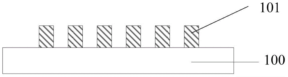
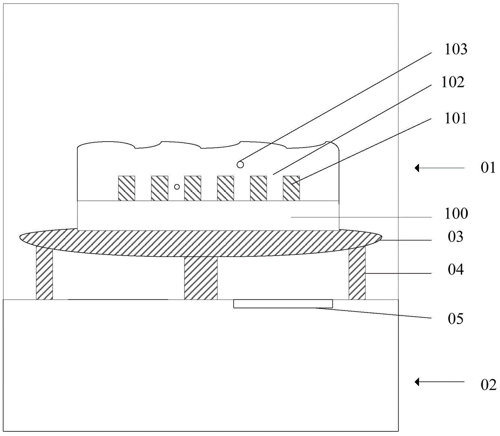
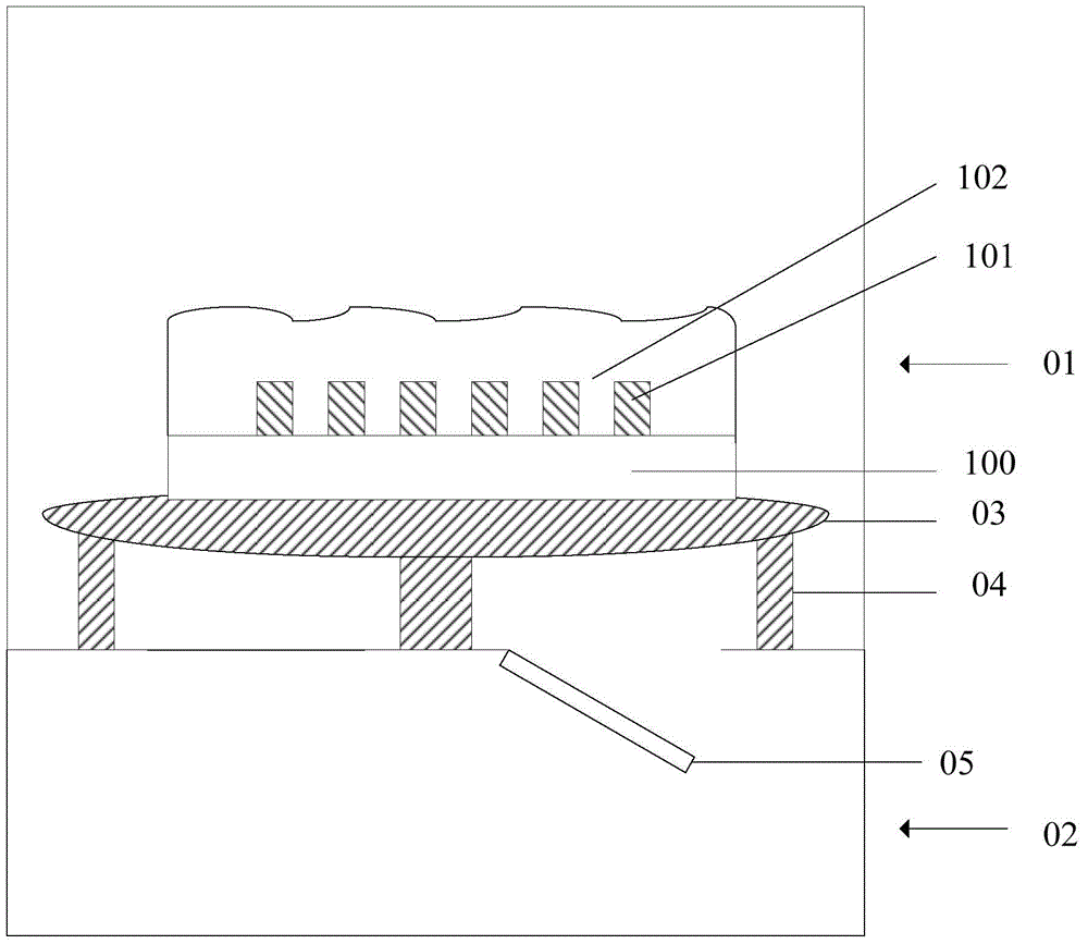
[0038] In the process of forming a photoresist material layer such as a planar layer or photoresist in the photolithography process, bubbles are easily formed in the planar layer or photoresist, and the bubbles in the planar layer or photoresist will affect the photolithography accuracy.

[0039] The cause of formation of bubbles in the analysis planar layer is as follows: coating organic solution in spin coating equipment, organic solution enters the nozzle of described spin coating equipment through conduit, easily produces bubbles in the organic solution in conduit because of reasons such as pressure, flow rate, in After the organic solution is coated on the surface of the wafer, bubbles may still exist in the organic solution; in addition, due to the continuous shrinking of the critical dimensions of semiconductor manufacturing, there are many small gaps on the surface of the wafer (such as gaps between gate bars) , when the organic solution is coated between these gaps, it...


PUM


Abstract

The invention provides a photoetching method and a processing chamber. The photoetching method comprises the following steps: putting a wafer into a coating chamber, setting the air pressure in the coating chamber to be first air pressure, carrying out first spinning on the wafer surface, and covering the wafer surface with a photoetching material layer; after carrying out first spinning, carrying out first depressurization step, and lowering the air pressure in the coating chamber into the second air pressure from the first air pressure; carrying out second spinning on the wafer surface; carrying out solidification treatment on the photoetching material layer; and photoetching the wafer covered with the photoetching material layer. The first depressurization step is carried out after first spinning is carried out on the wafer surface, so that bubbles in the photoetching material layer are extruded or broken off along with air pressure drop; the bubbles do not easily exist in the photoetching material layer which is subjected to second spinning and solidification treatment. Therefore, the photoetching accuracy can be effectively improved.

Description

technical field [0001] The invention relates to the field of semiconductors, in particular to a photolithography method and a process chamber. Background technique [0002] As the density of transistors on integrated circuits continues to increase, the critical dimensions (CD) of semiconductor manufacturing continue to shrink, and the requirements for lithographic precision are also increasing. [0003] In order to improve the precision of the photolithography process, before coating the photoresist, it is necessary to coat a flat layer on the surface of the wafer, so as to reduce the problem of the decrease of the precision of the photolithography caused by the unevenness of the wafer surface. The material of the flat layer is usually a highly viscous organic solution. In the prior art, the organic solution is coated with the same spin coating equipment as the photoresist coating, and the organic solution coated on the wafer is subsequently baked. A solid flat layer is for...

Claims


Application Information

Patent Timeline
IPC IPC(8): G03F7/00H01L21/027
Inventor 李高荣郑喆
Owner SEMICON MFG INT (SHANGHAI) CORP
Why Eureka
Try Eureka