A Circular Motion Method for Multiple Wafers Based on Multiple Exposure Programs

A cyclic motion, multi-exposure technology, applied in microlithography exposure equipment, photolithography process exposure devices, etc., can solve the problems of reducing the use efficiency of the machine, wasting machine time, consumption, etc., and reducing the time occupied by the machine. , reduce the size, reduce the effect of the exposure area

Active Publication Date: 2017-06-23
SHANGHAI HUALI MICROELECTRONICS CORP
View PDF5 Cites 0 Cited by
  • Summary
  • Abstract
  • Description
  • Claims
  • Application Information

AI Technical Summary

Problems solved by technology

This method has two defects: 1. It consumes machine time, because the silicon wafers in the silicon wafer box need to be transferred to the silicon wafer carrier stage one by one, therefore, a lot of time is needed to be consumed on the silicon wafer transmission, which reduces the operating time of the machine. Use efficiency; 2. The effect of taking away the particles is relatively poor. After the silicon wafer is passed back to the silicon wafer box through one round of exposure, the silicon wafer is exposed again when the next round of silicon wafer exposure is carried out. The wafer itself already has particles. After multiple rounds of exposure, the particles of the silicon wafer itself accumulate more and more, resulting in a poor effect of taking away the particles.

Method used


Image

  • A Circular Motion Method for Multiple Wafers Based on Multiple Exposure Programs
  • A Circular Motion Method for Multiple Wafers Based on Multiple Exposure Programs
  • A Circular Motion Method for Multiple Wafers Based on Multiple Exposure Programs

Examples


Embodiment Construction

[0025] In order to make the purpose, technical solution and advantages of the present invention clearer, the following will further describe the implementation of the present invention in detail in conjunction with the accompanying drawings. Those skilled in the art can easily understand other advantages and effects of the present invention from the contents disclosed in this specification. The present invention can also be implemented or applied through other different specific implementation modes, and various modifications or changes can be made to the details in this specification based on different viewpoints and applications without departing from the spirit of the present invention.

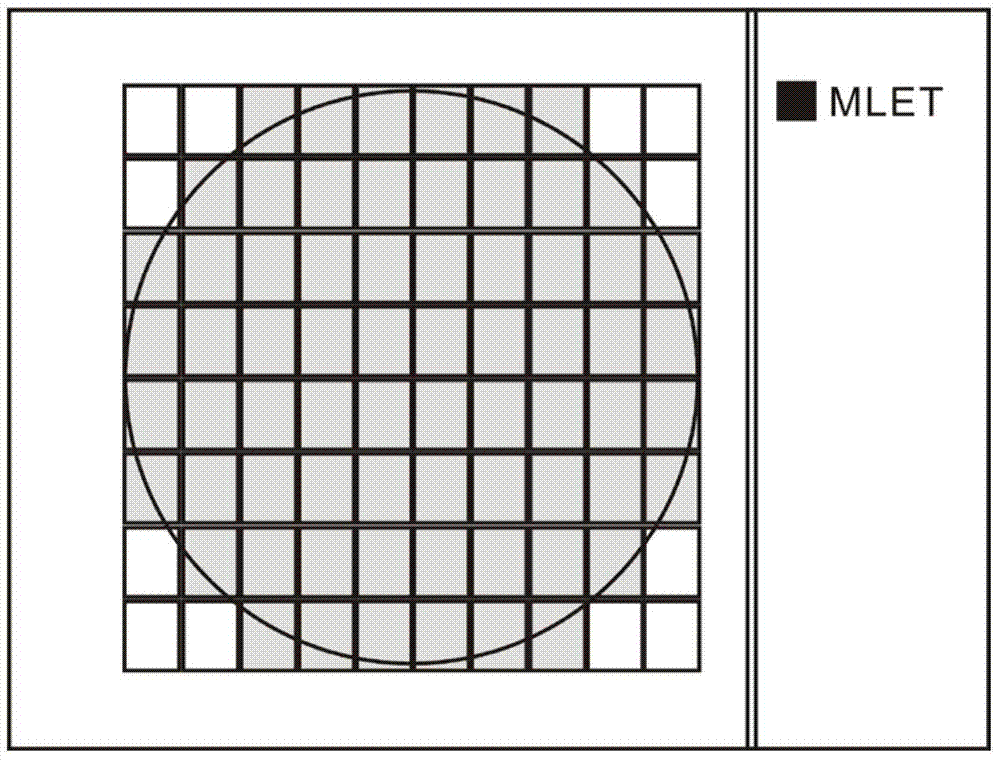
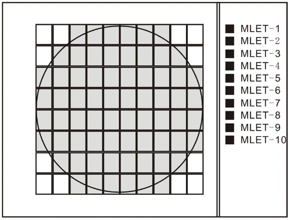
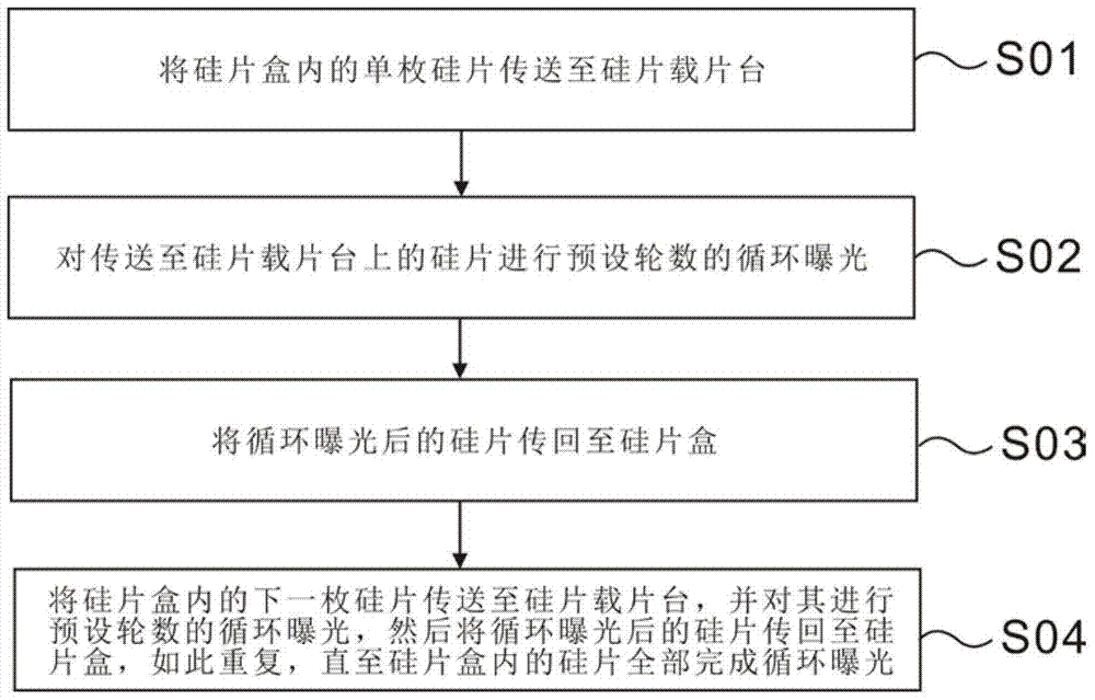
[0026] The above and other technical features and beneficial effects will be combined with the embodiments and the accompanying image 3 , 4 The multi-silicon wafer circular movement method based on the multi-exposure program of the present invention is described in detail. image 3 It i...


PUM


Abstract

The invention discloses a multi-exposure-program based multi-silicon-wafer circulation movement method, comprising the following steps of firstly transferring a single silicon wafer in a silicon wafer box to a silicon wafer carrying table; next, performing circulation exposure on the silicon wafer transferred to the silicon wafer carrying table at a preset number of rounds; then transferring the silicon wafer after being circularly exposed back to the silicon wafer box; and finally performing circulation exposure on the next silicon wafer in the silicon wafer box with the preset number of rounds until all the silicon wafers in the silicon wafer box are circularly exposed. According to the multi-exposure-program based multi-silicon-wafer circulation movement method, by changing the circulation exposure sequences of the silicon wafers, the occupied time on the machine table in transferring the silicon wafers is reduced; meanwhile, the method has a better effect on taking away fine particles from ultra-pure water to enable the fine particles in the ultra-pure water to be accumulated on the single silicon wafer until reaching a saturation condition, so that the fine particles in the ultra-pure water is less and less; and meanwhile, by reducing the exposure area of the silicon wafers, the sizes of flatness result files produced by each exposure image can be reduced, so that the problem of machine table downtime caused by overlarge flatness result files is solved.

Description

technical field [0001] The invention belongs to the technical field of semiconductor photolithography technology, and relates to a multi-silicon wafer circular motion method based on multi-exposure programs. Background technique [0002] In semiconductor technology, the essence of photolithography is to copy the temporary circuit structure to the silicon wafer that will be etched and ion-implanted later. Photolithography uses light-sensitive photoresist materials and controlled exposure to create three-dimensional patterns on the surface of silicon wafers. [0003] An important performance indicator in lithography is the resolution of each pattern. To improve resolution, more advanced immersion lithography was developed. In traditional lithography technology, the medium between the projection lens of the lithography machine and the photoresist on the silicon wafer is air. [0004] Immersion lithography refers to a new type of lithography that fills the gap between the pro...

Claims


Application Information

Patent Timeline
Patent Type & Authority Patents(China)
IPC IPC(8): G03F7/20
Inventor 李文亮吴鹏陈力钧朱骏莫少文
Owner SHANGHAI HUALI MICROELECTRONICS CORP
Why Eureka
Try Eureka