Production control method, device and system of a thin film electronic device

A production control method and technology for electronic devices, applied in the direction of electrical components, semiconductor/solid-state device testing/measurement, circuits, etc., can solve problems such as increased production costs, small scope of modification, inability to achieve circuit pattern modification, etc., and reduce corrections. cost effect

Active Publication Date: 2018-06-19
SHENZHEN SHENGDEJIN TECH CO LTD
View PDF4 Cites 0 Cited by
  • Summary
  • Abstract
  • Description
  • Claims
  • Application Information

AI Technical Summary

Problems solved by technology

However, laser equipment is not a conventional equipment for manufacturing thin-film electronic devices, and additional purchase is required, resulting in increased production costs
At the same time, laser fusing can usually only target one point at a time, and the scope of modification is small, which cannot achieve the purpose of modifying large-area circuit patterns, and the efficiency of circuit pattern correction is not high
Moreover, the accuracy of laser fusing is insufficient, and it is impossible to control the high-precision fine-tuning process

Method used


Image

  • Production control method, device and system of a thin film electronic device
  • Production control method, device and system of a thin film electronic device
  • Production control method, device and system of a thin film electronic device

Examples


Embodiment 1

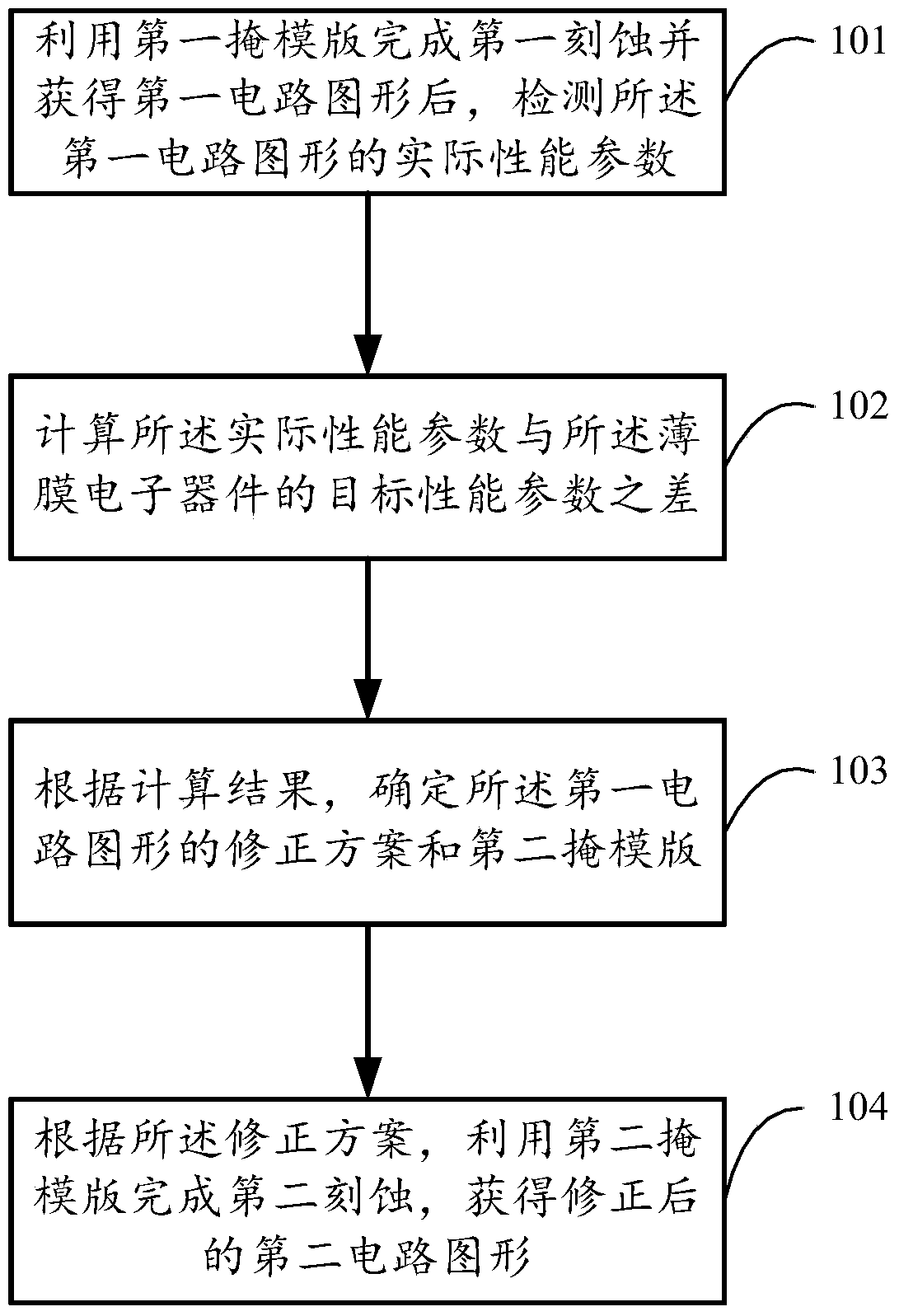
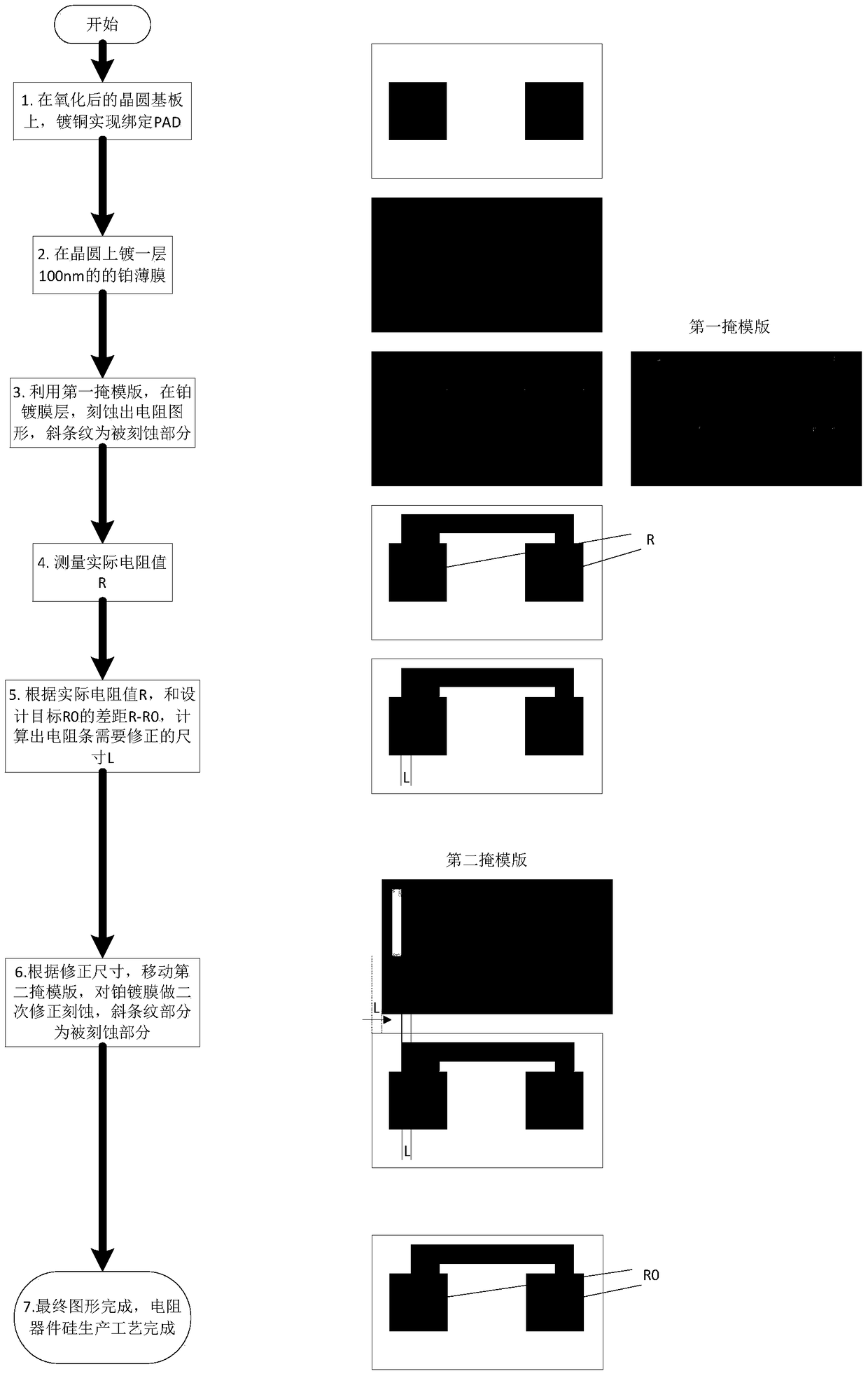
[0085] Apply the production control method of the above-mentioned thin-film electronic device to the following scenario, that is, the thin-film electronic device to be produced is a resistor, and the target resistance value should be R0, and the actual resistance value R of the first circuit pattern obtained after the first etching is . image 3 A schematic diagram of the circuit diagram of the production flow of the resistor and the corresponding thin film electronic device for each step by applying the production control method provided by the present invention. The production process includes:

[0086] 1. On the oxidized wafer substrate, copper plating is used to bond the PAD;

[0087] 2. Coating a layer of 100nm platinum film on the wafer;

[0088] 3. Use the first mask to etch the resistance pattern on the platinum coating layer, and the oblique stripes are the etched parts;

[0089] 4. Measure the actual resistance value R;

[0090] 5. According to the difference R-R...


PUM


Abstract

The invention discloses production control method, device and system of a thin-film electronic device. The method comprises the following steps of: finishing first etching by using a first mask template and detecting an actual performance parameter of a first circuit pattern after obtaining the first circuit pattern; calculating the difference between the actual performance parameter and a target performance parameter of the thin-film electronic device; determining a correction scheme of the first circuit pattern and a second mask template according to a calculation result; and finishing second etching by using the second mask template according to the correction scheme, and acquiring a corrected second circuit pattern.

Description

technical field [0001] The invention relates to the field of semiconductor production, in particular to a production control method, device and system for thin film electronic devices. Background technique [0002] High-precision thin-film electronic devices need to rely on the thickness of the film to ensure the accuracy of the device's operating characteristics during manufacture. However, common coating equipment can only guarantee a thickness accuracy of -5% to +5% at most. If the device operating characteristic accuracy is higher than the coating thickness control accuracy, the device production yield will be too low, or it will not be able to be produced. [0003] Therefore, the current thin-film electronic devices often use laser to fuse metal or polysilicon after the production is completed, so as to achieve the purpose of correcting the circuit pattern, and then obtain the target operating characteristics of the thin-film electronic device. However, laser equipment...

Claims


Application Information

Patent Timeline
Patent Type & Authority Patents(China)
IPC IPC(8): H01L21/66
CPCH01L22/20
Inventor 孙轶群
Owner SHENZHEN SHENGDEJIN TECH CO LTD
Why Eureka
Try Eureka