Three-dimensional laminated semiconductor structure and manufacturing method thereof

A semiconductor and stacking technology, which is applied in semiconductor/solid-state device manufacturing, semiconductor devices, electric solid-state devices, etc., can solve problems such as bending and collapse of composite layer columns

Active Publication Date: 2015-11-25
MACRONIX INT CO LTD
View PDF8 Cites 10 Cited by
  • Summary
  • Abstract
  • Description
  • Claims
  • Application Information

AI Technical Summary

Problems solved by technology

The manufacturing method of the embodiment solves the problem of bending and/or collapse of t

Method used


Image

  • Three-dimensional laminated semiconductor structure and manufacturing method thereof
  • Three-dimensional laminated semiconductor structure and manufacturing method thereof
  • Three-dimensional laminated semiconductor structure and manufacturing method thereof

Examples


Embodiment Construction

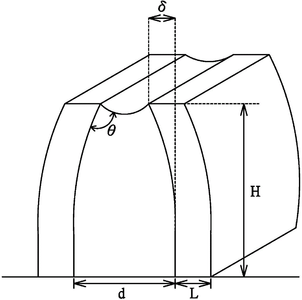
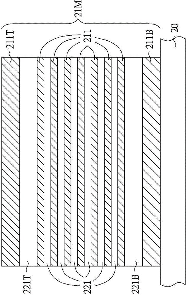
[0058]In the embodiments of the present invention, a method for manufacturing a three-dimensional stacked semiconductor structure and the resulting structure are proposed. In the manufacturing method of the three-dimensional stacked semiconductor structure proposed in the embodiment, a multi-layer (amulti-layer) includes a plurality of first dielectric layers and a plurality of second dielectric layers alternately stacked on a substrate, and then patterned Composite layers to form a plurality of first patterned stacks and a plurality of spaces between the first patterned stacks. In an embodiment, the first dielectric layer is compressive layers with compressive stress, and the second dielectric layer is tensile layers with tensile stress. A portion of the second dielectric layer of one of the first patterned stacks is then removed, and the removed portion is replaced with a conductor. The three-dimensional stacked semiconductor structure manufactured by the manufacturing meth...


PUM


Abstract

The invention discloses a three-dimensional laminated semiconductor structure and a manufacturing method thereof. In the manufacturing method, a composite layer is formed on a substrate and is formed by alternate lamination of a plurality of first dielectric layer and a plurality of dielectric layers; and afterwards, the composite layer is patterned to form a plurality of first patterned laminates and a plurality of intervals between the first patterned laminates, one of the first patterned laminates has a width F0, and one of the intervals has a width Fs. In an embodiment, the width F0 is equal to or greater than two times of the width Fs. Then, part of the second dielectric layers of one of the first patterned laminates are removed, so that a plurality of first cavities are formed in the first patterned laminate. Afterwards, first conductors are filled in the first cavities of the first patterned laminate.

Description

technical field [0001] The present invention relates to a three-dimensional stacked semiconductor structure and its manufacturing method, and in particular to a three-dimensional stacked semiconductor structure with a dielectric support between multi-layered pillars and its method of manufacture. Background technique [0002] A great feature of non-volatile memory element design is the ability to preserve the integrity of the data state when the memory element loses or removes power. Currently, many different types of non-volatile memory devices have been proposed in the industry. However, related companies are still developing new designs or combining existing technologies to stack memory cell planes to achieve a memory structure with higher storage capacity. For example, some three-dimensional stacked NAND gate (NAND) flash memory structures have been proposed. However, there are still some problems to be solved in the conventional 3D stacked memory structure. [0003]...

Claims


Application Information

Patent Timeline
IPC IPC(8): H01L21/8247H01L27/115
Inventor 赖二琨
Owner MACRONIX INT CO LTD
Why Eureka
Try Eureka