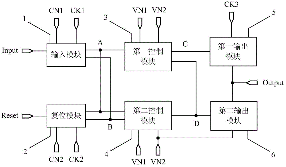
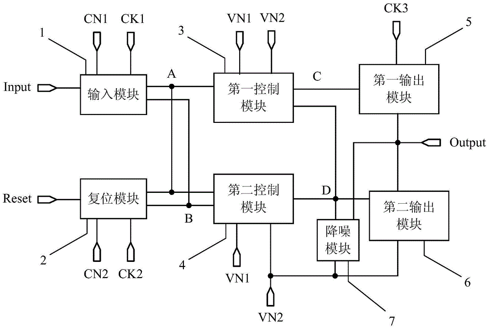
Shifting register and driving method thereof as well as gate drive circuit and display device
A technology for shift registers and gates, which is applied in the field of gate drive circuits, display devices, and shift registers. It can solve the problems of unstable gate potential, affecting the stable output of shift registers, and large noise in scanning signals.
- Summary
- Abstract
- Description
- Claims
- Application Information
AI Technical Summary
Problems solved by technology
Method used
Image
Examples
example 1
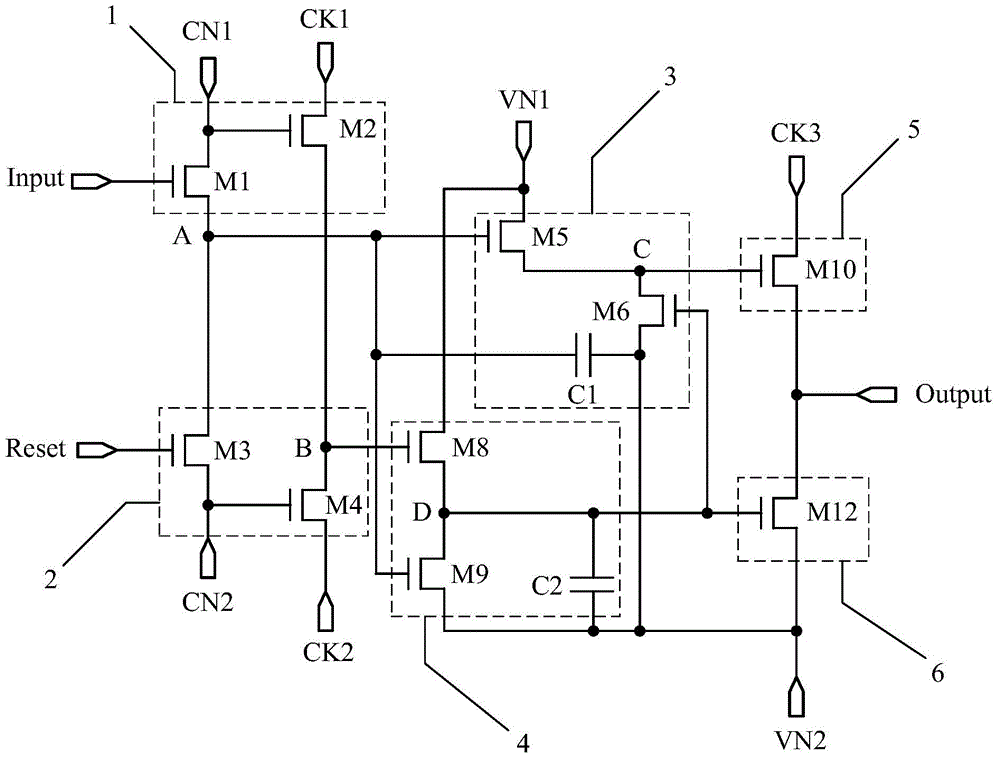
[0126] by Figure 2a The structure of the shift register shown is taken as an example to describe its working process, in which Figure 2aIn the shift register shown, all the switch transistors are N-type switch transistors, and each N-type switch transistor is turned on under the action of a high potential, and is turned off under the action of a low potential; the potential of the first direct current signal vn1 is a high potential, The potential of the second DC signal vn2 is low potential; the potential of the first reference signal cn1 is high potential, and the potential of the second reference signal cn2 is low potential; the corresponding input and output timing diagram is as follows Figure 4a shown. Specifically, choose the Figure 4a There are four stages in the input and output timing diagram shown: input stage S1, output stage S2, reset stage S3 and reset hold stage S4.
[0127] In the input phase S1, ck1=0, ck3=0, input=1, reset=0.
[0128] Since reset=0, the...
example 2
[0138] by Figure 3a The structure of the shift register shown is taken as an example to describe its working process, in which Figure 3a In the shift register shown, all the switch transistors are N-type switch transistors, and each N-type switch transistor is turned on under the action of a high potential, and is turned off under the action of a low potential; the potential of the first direct current signal vn1 is a high potential, The potential of the second DC signal vn2 is low potential; the potential of the first reference signal cn1 is high potential, and the potential of the second reference signal cn2 is high potential; the corresponding input and output timing diagram is as follows Figure 4b shown. Specifically, choose the Figure 4b There are four stages in the input and output timing diagram shown: input stage S1, output stage S2, reset stage S3 and reset hold stage S4.
[0139] In the four phases of input phase S1, output phase S2, reset phase S3 and reset h...
PUM
 Abstract
Description
Claims
Application Information


