A circuit board and display device
A technology for circuit boards and display substrates, used in printed circuits, printed circuits, printed circuit manufacturing, etc., can solve the problems of high cost, long disassembly time, insufficient monitoring frequency, etc., to improve product quality, reduce product risks, The effect of reducing the risk of binding
- Summary
- Abstract
- Description
- Claims
- Application Information
AI Technical Summary
Problems solved by technology
Method used
Image
Examples
Embodiment 1
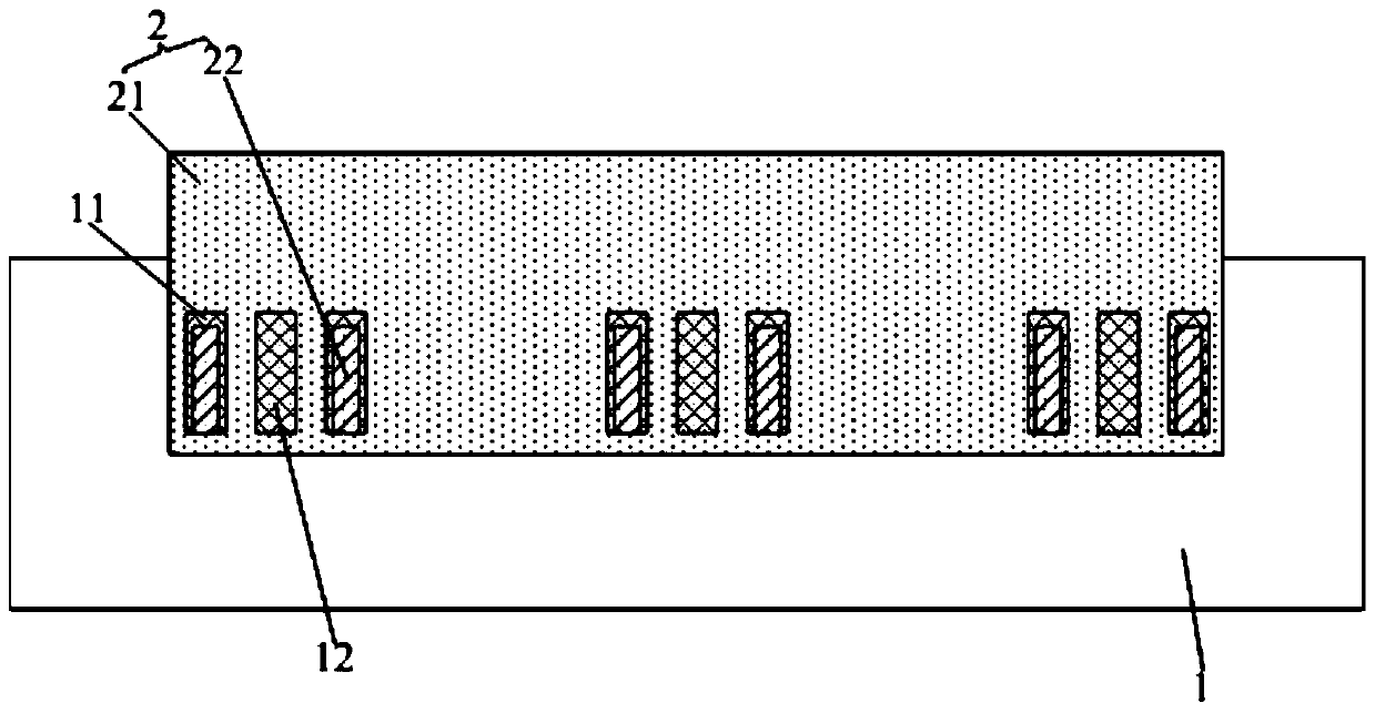
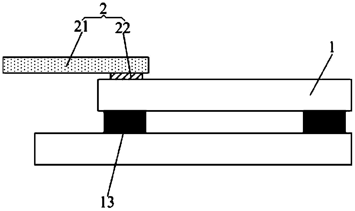
[0028] This embodiment provides a circuit board, such as figure 2 As shown, it is used for binding connection on the display substrate 1, including a binding connection terminal 2, the binding connection terminal 2 includes a base film 21 and a plurality of first terminals 22 arranged on the base film 21, the base film 21 corresponds to The area of the first terminal 22 includes a transparent film material, wherein a part of the base film 21 corresponding to the first terminal 22 is made of a transparent film material.
[0029] By making the region of the first connection terminal 22 of the corresponding part of the base film 21 of the binding connection end 2 adopt a transparent film material, it is possible to pass through the transparent base film 21 when the binding state of the binding connection end 2 is monitored. Directly observe the binding state of the binding state, so as to realize the changing state of the gold ball particles after binding, the coincidence of t...
Embodiment 2
[0037] This embodiment provides a circuit board, which is different from Embodiment 1, such as Figure 4 As shown, a plurality of first terminals 22 are arranged in a row, and all areas of the base film 21 corresponding to the row of first terminals 22 are made of transparent film materials.
[0038] With such an arrangement, the binding conditions of all the first terminals 22 and the second terminals on the display substrate 1 can be observed through the base film 21, ensuring that the binding conditions of each binding terminal can be observed, thereby further improving the binding The monitoring level of product quality in the process reduces product risk and improves product quality.
[0039] In this embodiment, the row of first terminals 22 is used for corresponding binding connection with a row of second terminals on the display substrate 1; a third terminal 12 is also provided in a part of the interval area of the row of second terminals, Part of the interval area b...
Embodiment 3
[0044] This embodiment provides a display device, including the circuit board in any one of Embodiments 1-2.
[0045] By adopting the circuit board in any one of Embodiments 1-2, the monitoring level of the binding quality of the display device is improved, the binding risk of the display device is reduced, and the quality of the display device is improved without affecting the quality of the display device. The structure and photoelectric characteristics of the display device.
[0046] The display device may be any product or component with a display function such as a mobile phone, a tablet computer, a television, a monitor, a notebook computer, a digital photo frame, a navigator, and the like.
PUM
 Abstract
Description
Claims
Application Information


