Manufacturing method of array substrate

A manufacturing method and technology of array substrates, which are applied in semiconductor/solid-state device manufacturing, semiconductor devices, electrical components, etc., can solve problems such as easy peeling off of organic film layers, increase roughness and cleanliness, solve easy peeling off, and avoid TEG unusual effect

Active Publication Date: 2018-09-18
WUHAN CHINA STAR OPTOELECTRONICS TECH CO LTD
View PDF6 Cites 0 Cited by
  • Summary
  • Abstract
  • Description
  • Claims
  • Application Information

AI Technical Summary

Problems solved by technology

[0005] The purpose of the present invention is to provide a method for manufacturing an array substrate to solve the technical problem that the organic film layer is easy to fall off in the prior art

Method used


Image

  • Manufacturing method of array substrate
  • Manufacturing method of array substrate

Examples


Embodiment Construction

[0031] The implementation of the present invention will be described in detail below in conjunction with the accompanying drawings and examples, so as to fully understand and implement the process of how to apply technical means to solve technical problems and achieve technical effects in the present invention. It should be noted that, as long as there is no conflict, each embodiment and each feature in each embodiment of the present invention can be combined with each other, and the formed technical solutions are all within the protection scope of the present invention.

[0032] Embodiments of the present invention provide an array substrate and a manufacturing method thereof.

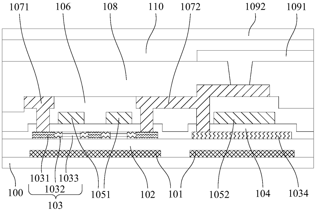
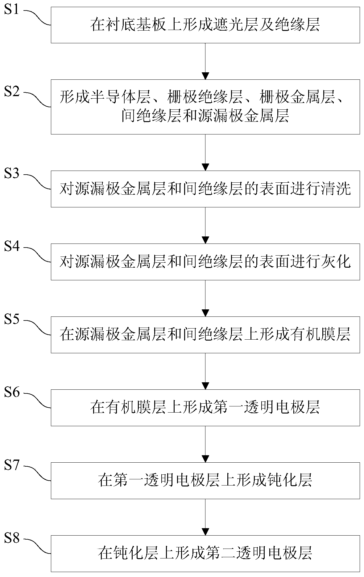
[0033] Embodiments of the present invention are described by taking an array substrate manufactured by a Low Temperature Poly-silicon (LTPS for short) process as an example. Such as figure 1 As shown, the array substrate mainly includes a light-shielding layer 101, an insulating layer 102, a semicond...


PUM


Abstract

The invention discloses a manufacturing method of an array substrate, belongs to the technical field of display, and solves the technical problems in the prior art that an organic film layer is liable to fall off. The manufacturing method of the array substrate comprises the steps that a semiconductor layer, a gate electrode insulating layer, a gate electrode metal layer, an interlayer insulating layer and a source and drain electrode metal layer are formed; the surface of the source and drain electrode metal layer and the interlayer insulating layer is cleaned; ashing is performed on the surface of the source and drain electrode metal layer and the interlayer insulating layer; and the organic film layer is formed on the source and drain electrode metal layer and the interlayer insulating layer.

Description

technical field [0001] The present invention relates to the field of display technology, in particular, to a method for manufacturing an array substrate. Background technique [0002] With the development of display technologies, liquid crystal displays have become the most common display devices. Among them, the array substrate is an important part of the liquid crystal display. [0003] Thin Film Transistor (TFT for short) arrays, scan lines, data lines, common electrode lines, pixel electrodes, common electrodes, and multiple insulating layers are arranged on the array substrate to realize the driving of liquid crystals during the display process. [0004] The manufacturing process of the array substrate mainly forms various layer structures through multiple mask patterning processes. Each layer structure in the array substrate mainly includes a semiconductor layer, a gate insulating layer, a gate metal layer, an inter-insulating layer (ILD), a source-drain metal layer,...

Claims


Application Information

Patent Timeline
Patent Type & Authority Patents(China)
IPC IPC(8): H01L27/12H01L21/02
Inventor 杨元隆
Owner WUHAN CHINA STAR OPTOELECTRONICS TECH CO LTD
Why Eureka
Try Eureka