Hybrid imaging detector pixel structure with step supports and preparation method of hybrid imaging detector pixel structure

An imaging detector and pixel structure technology, applied in the field of microelectronics, can solve the problems of large alignment deviation of infrared image parts and visible light image parts, affecting imaging quality, etc., to improve the quality of hybrid imaging, improve quality, and reduce volume. Effect

Active Publication Date: 2015-12-30
SHANGHAI INTEGRATED CIRCUIT RES & DEV CENT
View PDF4 Cites 11 Cited by
  • Summary
  • Abstract
  • Description
  • Claims
  • Application Information

AI Technical Summary

Problems solved by technology

[0003] However, in the existing hybrid imaging devices, lenses are used to form two optical paths to sense and image visible light and infrared light respectively, and finally a computer processing system is used to

Method used


Image

  • Hybrid imaging detector pixel structure with step supports and preparation method of hybrid imaging detector pixel structure
  • Hybrid imaging detector pixel structure with step supports and preparation method of hybrid imaging detector pixel structure
  • Hybrid imaging detector pixel structure with step supports and preparation method of hybrid imaging detector pixel structure

Examples


Embodiment Construction

[0042] In order to make the content of the present invention clearer and easier to understand, the content of the present invention will be further described below in conjunction with the accompanying drawings. Of course, the present invention is not limited to this specific embodiment, and general replacements known to those skilled in the art are also covered within the protection scope of the present invention.

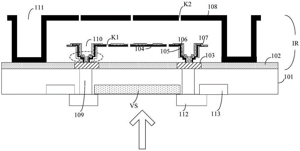
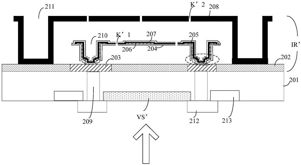
[0043] The pixel structure of the visible light and infrared hybrid imaging detector of the present invention includes: a wafer used as a filter layer for filtering out visible light, a visible light sensing area located on the lower surface of the wafer, a dielectric layer and an infrared sensing area located on the upper surface of the wafer area, a supporting component, and a conversion unit for calculating and converting the electrical signals output by the visible light sensing area and the infrared sensing area into an image; wherein, the visible light sensing...


PUM


Abstract

The invention provides a hybrid imaging detector pixel structure with step supports and a preparation method of the hybrid imaging detector pixel structure. The hybrid imaging detector pixel structure comprises a wafer, a visible light induction region located at the lower surface of the wafer, an infrared induction region located at the upper surface of the wafer and a conversion unit which is used for calculating electric signals outputted by the visible light induction region and the infrared induction region and converting the electric signals into an image; the infrared induction region includes contact trench structures which are located in a dielectric layer, infrared induction structures which are provided with multiple-step-shaped side walls, and a supporting component which is located at around the infrared induction structures and does not contact with the infrared induction structures; a first cavity is formed between the infrared induction structures and the upper surface of the dielectric layer; the bottom of the supporting component is connected with the dielectric layer; release holes are formed in the top of the supporting component; the inner surface of the supporting component is provided with an infrared reflective material or the whole supporting component is made of an infrared reflective material; and a second cavity is formed between the support component and the infrared induction structures.

Description

technical field [0001] The invention relates to the technical field of microelectronics, in particular to a visible-infrared hybrid imaging detector pixel structure with step support and a preparation method thereof. Background technique [0002] With the development of industry and living standards, pure infrared imaging or pure visible light imaging can no longer meet the demand. Imaging technologies with wider wavelength bands have attracted more and more attention, especially imaging technologies that are sensitive to visible light and infrared light at the same time. [0003] However, in existing hybrid imaging devices, lenses are used to form two optical paths to sense and image visible light and infrared light respectively, and finally a computer processing system is used to synthesize them together. Due to the separation of the optical paths, the formed infrared image part and visible light image Some of them have large alignment deviations, which seriously affect th...

Claims


Application Information

Patent Timeline
IPC IPC(8): H01L27/146
Inventor 康晓旭赵宇航
Owner SHANGHAI INTEGRATED CIRCUIT RES & DEV CENT
Why Eureka
Try Eureka