Apparatus and method for generating three-layer plasma photonic crystal
A plasma and photonic crystal technology, which is applied in the field of plasma application technology and optics, can solve the problems of limited application fields and application prospects, limited wavelength bands, and insufficient modulation methods, so as to achieve diversified modulation of beams, widened wavelength bands, and a wide range of Effects of application areas and application prospects
- Summary
- Abstract
- Description
- Claims
- Application Information
AI Technical Summary
Problems solved by technology
Method used
Image

Examples
Embodiment 1
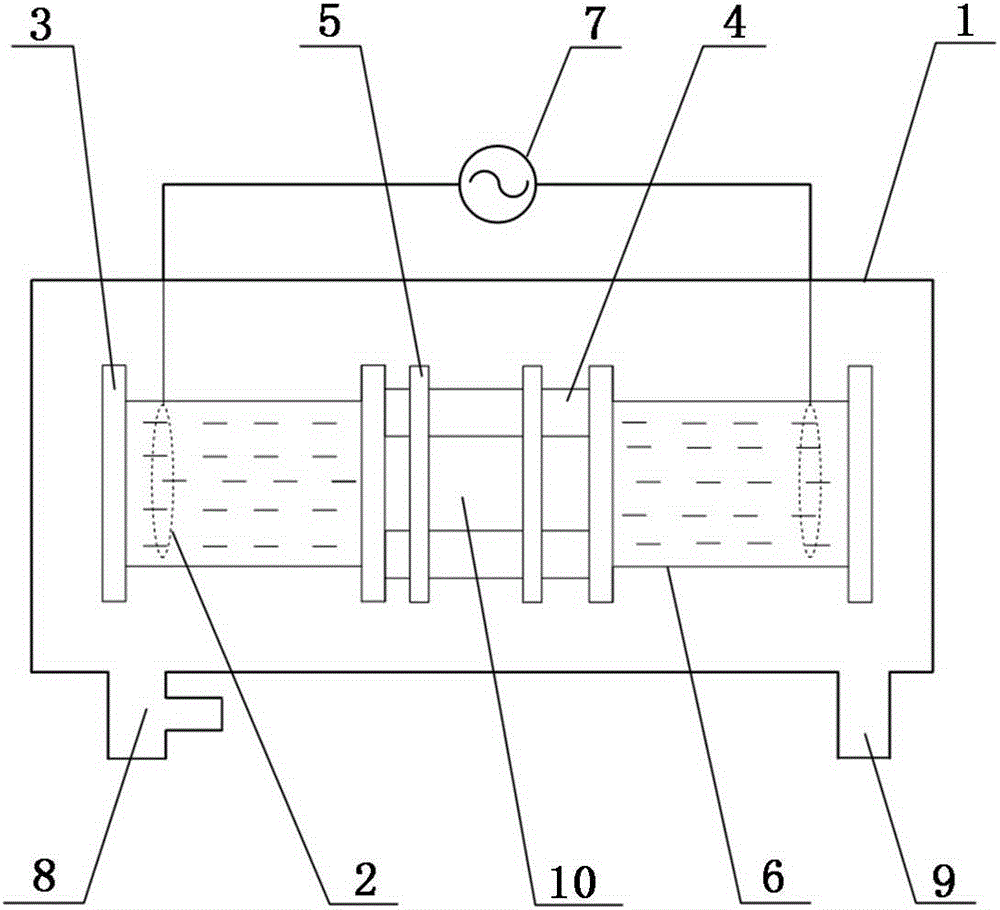
[0035] like figure 1 As shown, the device for producing three layers of plasma photonic crystals provided by the present invention is to symmetrically arrange two airtight dielectric containers in a horizontal cylindrical vacuum reaction chamber 1, and inject water into the airtight dielectric containers to form two Water electrode6. The two water electrodes 6 are electrically connected to a plasma generating power source 7 . The water electrode 6 is made of a plexiglass tube which is sealed by quartz glass baffles 3 at both ends. The plexiglass tube is filled with water, and a copper ring 2 is set in the plexiglass tube. The two copper rings 2 are respectively electrically connected to the positive pole and the negative pole of the plasma generation power supply 7 outside the vacuum reaction chamber 1 through power lines. The thickness of the quartz glass block 3 is between 0.1 mm and 5 mm.
[0036] The space between the two water electrodes 6 is a discharge gap 10 , and t...
Embodiment 2
[0040] The method for producing three layers of plasma photonic crystal provided by the present invention comprises the following steps:
[0041] a. A vacuum reaction chamber 1 is provided, an air inlet 8 and an air outlet 9 are provided on the wall of the vacuum reaction chamber 1 , and two water electrodes 6 are installed in the vacuum reaction chamber 1 . The water electrode 6 adopts a plexiglass tube sealed with quartz glass baffles 3 on both sides and filled with water, and a built-in copper ring 2 is electrically connected with the plasma generating power supply 7 .
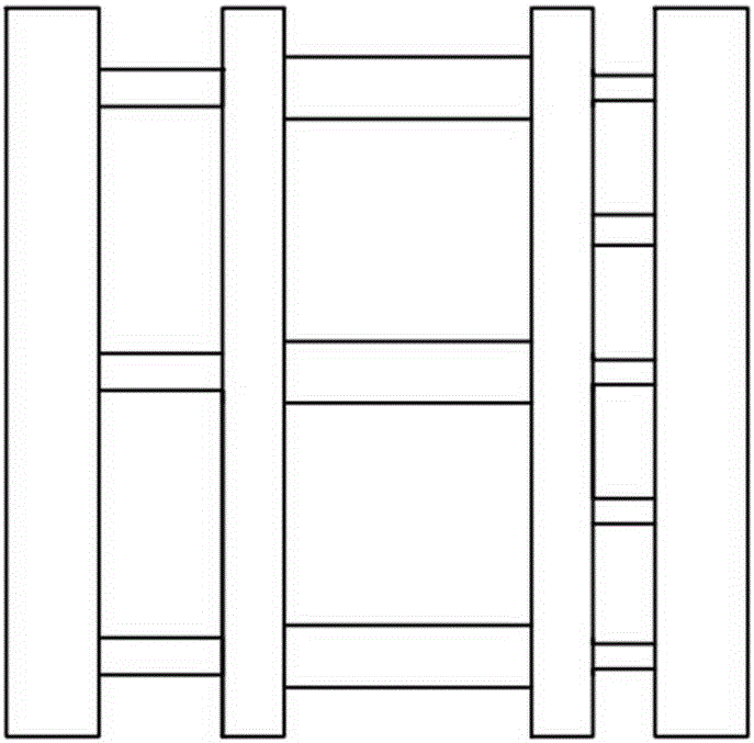
[0042] b. Between the two water electrodes 6, three frames 4 with different thicknesses are arranged side by side as the boundary of the discharge gap, and the thickness of the frames 4 is between 1 mm and 10 mm; a dielectric plate is arranged between two adjacent frames 4 5. Two dielectric plates 5 divide the discharge gap 10 into a three-layer structure. The frame 4 and the dielectric plate 5 are respect...
Embodiment 3
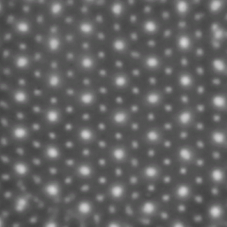
[0047] Compared with Example 2, the specific experimental parameters of this embodiment are: the thickness of the quartz glass baffle 3 is 1.5 mm, the thickness of the quartz dielectric plate 5 is 1 mm, and the thicknesses of the three quadrangular glass frames 4 are respectively 2 mm, 2 mm and 1 mm from left to right. 4mm and 1mm, the vacuum reaction chamber 1 is pure air, the air pressure is 0.4 atmospheres, the frequency of the plasma generating power supply 7 is 60kHz, and the peak voltage is 5.2kV.
[0048] The pattern photo (i.e. the end view) and the side view of the three-layer plasmonic photonic crystal produced in this embodiment are respectively as follows figure 2 and image 3 shown. Depend on figure 2 It can be seen that the bright spots are arranged in a hexagonal structure, and there is a bright spot in the center of each hexagon; the dark spots are distributed around each bright spot, and the dark spots are also arranged in a hexagonal structure; the diamet...
PUM
| Property | Measurement | Unit |
|---|---|---|
| Thickness | aaaaa | aaaaa |
| Thickness | aaaaa | aaaaa |
| Thickness | aaaaa | aaaaa |
Abstract
Description
Claims
Application Information
 - R&D
- Intellectual Property
- Life Sciences
- Materials
- Tech Scout
- Unparalleled Data Quality
- Higher Quality Content
- 60% Fewer Hallucinations
Browse by: Latest US Patents, China's latest patents, Technical Efficacy Thesaurus, Application Domain, Technology Topic, Popular Technical Reports.
© 2025 PatSnap. All rights reserved.Legal|Privacy policy|Modern Slavery Act Transparency Statement|Sitemap|About US| Contact US: help@patsnap.com