
Eureka
For R&D, Eureka makes reading and utilizing patents & technical documents easy.
Eureka AIR
Designed for self-driven R&D workflows. Generate viable solutions, solve complex R&D challenges, empower your innovation with AI.

Eureka Materials
Designed for material experts only. Revolutionize your material R&D, from search, analyze, to developing new materials.

TechResearch
Generate reliable direction feasibility study reports for your R&D in just a few steps.

TechSeek
Discover and master advanced knowledge NOW. Basics, ideas, possibilities, all at once.

TechMind
As an expert in R&D Theories, TechMind can generates customized viable solutions instantly.

TechRisk
Analyze your overall solution with one click, know your potential R&D risks in advance.

TechMonitor
Get weekly tech updates, stay abreast of the latest tech innovations and key insights.
Display and organic light-emitting diode device thereof
A technology for light-emitting diodes and displays, which is applied to organic semiconductor devices, electric solid-state devices, semiconductor devices, etc., can solve problems such as low light extraction efficiency, and achieve the effect of improving light extraction rate.
- Summary
- Abstract
- Description
- Claims
- Application Information
AI Technical Summary
Problems solved by technology
Method used
Image

Examples
Embodiment 1
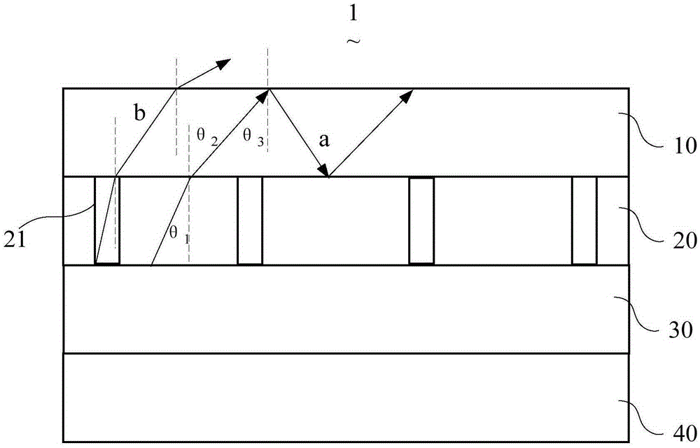
[0024] see figure 2 and image 3 , figure 2 It is a schematic structural diagram of an organic light emitting diode device in a preferred embodiment of the present invention, image 3 yes figure 2 A top view of the organic layer 30 of the OLED device is shown.
[0025] The OLED device 1 of this embodiment includes a glass substrate 10 , an anode layer 20 , an organic layer 30 and a cathode layer 40 stacked in sequence.
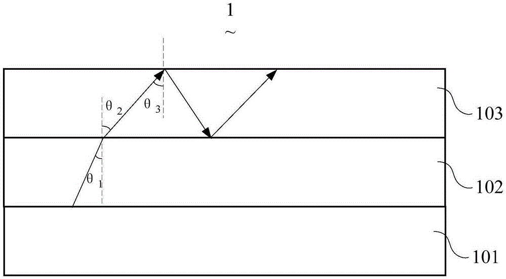
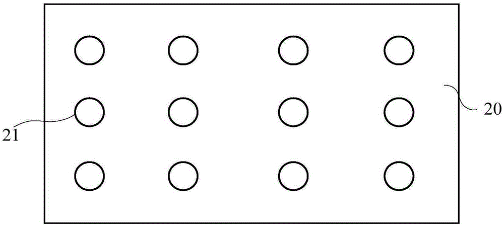
[0026] In this embodiment, electrons and holes are respectively injected from the cathode layer 40 and the anode layer 20, forming excitons in the organic layer 30 and exciting the material of the organic layer 30 to emit light, and the light excited from the organic layer 30 passes through the anode layer 20, and then emitted from the glass substrate 10. The refractive index n of the anode layer 20 1 greater than the refractive index n of the glass substrate 10 2 , wherein the anode layer 20 has a through hole 21 so that part of the light emitted by...
Embodiment 2
[0036] see Figure 4 , Figure 4 It is a schematic structural diagram of an organic light emitting diode device in another preferred embodiment of the present invention. The organic light emitting diode device 1 of this embodiment is substantially the same as that of the first embodiment, except that the organic light emitting diode device 1 in this embodiment is more A dielectric layer 50.
[0037] Specifically, the organic light emitting diode device 1 of this embodiment includes a glass substrate 10 , a dielectric layer 50 , an anode layer 20 , an organic layer 30 and a cathode layer 40 stacked in sequence.
[0038] The refractive index of the anode layer 20 in this embodiment is greater than the refractive index of the glass substrate 10, and the refractive index of the dielectric layer 50 is greater than the refractive index of the organic layer 30, wherein the anode layer 20 has a through hole 21 so that Part of the light emitted from the organic layer 30 directly ente...
PUM
 Abstract
Description
Claims
Application Information
 - R&D Engineer
- R&D Manager
- IP Professional
- Industry Leading Data Capabilities
- Powerful AI technology
- Patent DNA Extraction
Browse by: Latest US Patents, China's latest patents, Technical Efficacy Thesaurus, Application Domain, Technology Topic, Popular Technical Reports.
© 2024 PatSnap. All rights reserved.Legal|Privacy policy|Modern Slavery Act Transparency Statement|Sitemap|About US| Contact US: help@patsnap.com