Touch panel

A touch panel, cover substrate technology, applied in printed circuits, instruments, electrical digital data processing and other directions, can solve the problems of substrate deformation, substrate heating, heating temperature limitations, etc., to achieve thickness reduction, peeling prevention, flatness improved effect

Inactive Publication Date: 2016-01-27
LG INNOTEK CO LTD
View PDF0 Cites 5 Cited by
  • Summary
  • Abstract
  • Description
  • Claims
  • Application Information

AI Technical Summary

Problems solved by technology

However, the entire surface of the substrate may be heated when the joint is formed through a printing process
Therefore, since the entire surface of the substrate is heated, the substrate may be deformed
In particular, weakly heat-resistant materials such as polyethylene terephthalate (PET) may have limitations in heating temperature

Method used


Image

  • Touch panel
  • Touch panel
  • Touch panel

Examples


Embodiment Construction

[0044] In the following description of embodiments of the present invention, it will be understood that when a layer (or film), region, pattern or structure is referred to as being on another substrate, another layer (or film), another region, another solder When a pad or another pattern is "on" or "under", it may be "directly" or "indirectly" on other substrates, layers (or films), regions, pads or patterns, or there may also be one or more middle layer. Such positions of the layers are described with reference to the drawings.

[0045] The thickness and size of each layer (film), each region, each pattern or structure shown in the drawings may be exaggerated, omitted, or schematically drawn for the purpose of convenience or clarity. In addition, the size of elements does not utterly reflect an actual size.

[0046]Hereinafter, embodiments of the present invention will be described in detail with reference to the accompanying drawings.

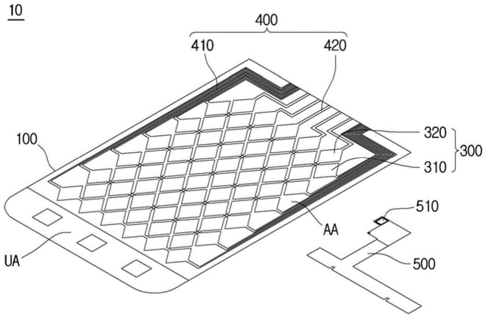
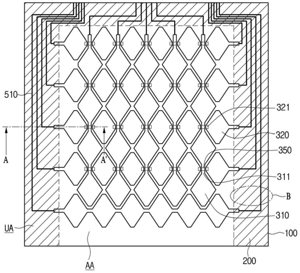
[0047] figure 1 is a perspective v...


PUM

PropertyMeasurementUnit
surface roughnessaaaaaaaaaa
thicknessaaaaaaaaaa
thicknessaaaaaaaaaa

Abstract

Provided is a touch panel including a cover substrate including an active area and an unactive area, and a printing layer on the unactive area. The printing layer has surface roughness in a range of 0.4 [mu] m to 0. 6 [mu] m. The printing layer has straightness in a range of +-0.1 [mu] m to +-10 [mu] m.

Description

technical field [0001] Embodiments of the present invention relate to touch panels. Background technique [0002] Recently, a touch panel that performs an input function by touching an image displayed on a display device with an input device such as a stylus or a finger has been applied to various electronic applications. [0003] The touch panel includes a cover substrate having an active area for sensing a position and a non-active area disposed at a peripheral portion of the active area. A printed layer may be provided in the non-active area. The printed layer may be printed with a material expressing a predetermined color such that the wire electrodes and a printed circuit board connecting the wire electrodes with an external circuit are not visible from the outside. [0004] The printing layer can be printed on the cover substrate by various schemes. In this case, deviations in surface roughness and flatness of the printed layer may affect reliability. For example, ...

Claims


Application Information

Patent Timeline
Patent Type & Authority Applications(China)
IPC IPC(8): G06F3/041
CPCG06F3/04164G06F3/0443G06F3/0446G06F3/03545G06F3/0412G06F3/047G06F2203/04101G06F2203/04107G06F2203/04111G06F2203/04112G06F2203/04808G06F2203/04809H05K1/0271H05K1/0274H05K2201/0145
Inventor 金洙根柳志昌许在鹤
Owner LG INNOTEK CO LTD
Why Eureka
Try Eureka