Automatic semiconductor wafer positioning device
An automatic positioning and semiconductor technology, which is applied in semiconductor/solid-state device manufacturing, electrical components, circuits, etc., can solve the problems of difficulty in meeting production requirements in precision and speed, failure of test work, waste of manpower and material resources, etc., and achieve automatic wafer alignment Accurate effect
- Summary
- Abstract
- Description
- Claims
- Application Information
AI Technical Summary
Problems solved by technology
Method used
Image

Examples
Embodiment Construction
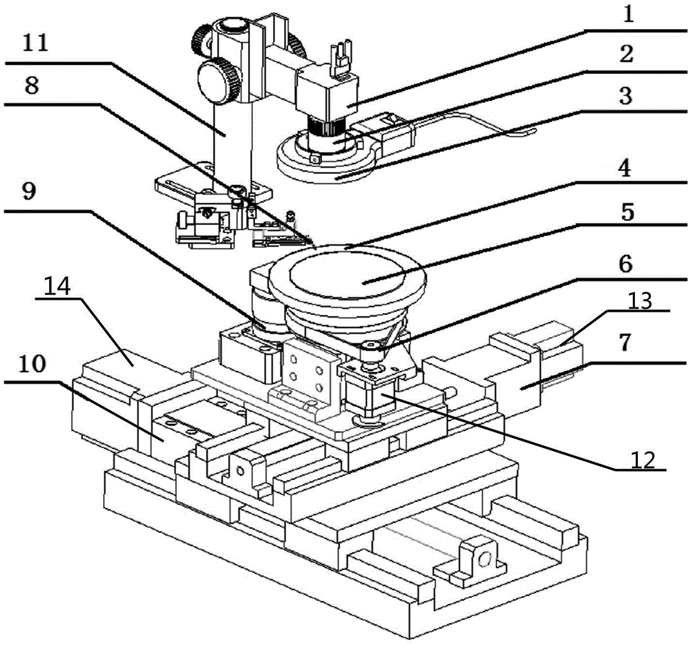
[0017] Such as figure 1 The semiconductor wafer automatic positioning device shown includes three parts: a vision system, a multi-directional mobile platform and a test probe. The vision system described in the present invention includes a camera, a microscope, and a light source; the vision system is used to extract wafer image features. The multi-directional mobile platform includes Y, X, Z, θ platforms, and the wafer stage 4 installed on the θ platform; the multi-directional mobile platform is used to control wafer movement. The test probes are used to make contact with the wafer. In the vision system of the present invention, the front end of the imaging lens of the camera 1 is sequentially installed with a microscope 2 and a light source 3 , and installed on the frame 11 through the camera 1 . In the present invention, the test probe 8 is aligned and contacted with the wafer 5, and the test probe 8 is integrally installed on the frame 11 of the vision system, and the re...
PUM
 Abstract
Description
Claims
Application Information
 - R&D
- Intellectual Property
- Life Sciences
- Materials
- Tech Scout
- Unparalleled Data Quality
- Higher Quality Content
- 60% Fewer Hallucinations
Browse by: Latest US Patents, China's latest patents, Technical Efficacy Thesaurus, Application Domain, Technology Topic, Popular Technical Reports.
© 2025 PatSnap. All rights reserved.Legal|Privacy policy|Modern Slavery Act Transparency Statement|Sitemap|About US| Contact US: help@patsnap.com