Solid-state imaging device and method for manufacturing solid-state imaging device

A technology of a solid-state imaging device and a manufacturing method, which is applied to electric solid-state devices, radiation control devices, transistors, etc., can solve the problems of shortened readout gate gate length, residual, photoelectric conversion elements and channel barriers, etc., To achieve the effect of suppressing afterimages

Inactive Publication Date: 2016-02-03
KK TOSHIBA
View PDF1 Cites 1 Cited by
  • Summary
  • Abstract
  • Description
  • Claims
  • Application Information

AI Technical Summary

Problems solved by technology

[0005] However, in recent solid-state imaging devices, as pixels have been miniaturized, the distance between the photoelectric conversion element and the floating diffusion region has narrowed, and the gate length of the readout gate has shortened accordingly. The potential barrier between
[0006] In a solid-state imaging device, if the potential barrier between the photoelectric conversion element and the channel becomes high, signal charges that should be transferred to the floating diffusion region may remain in the photoelectric conversion element without being transferred, resulting in afterimages in captured images.

Method used


Image

  • Solid-state imaging device and method for manufacturing solid-state imaging device
  • Solid-state imaging device and method for manufacturing solid-state imaging device
  • Solid-state imaging device and method for manufacturing solid-state imaging device

Examples


Embodiment Construction

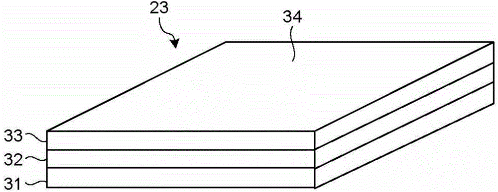
[0018] According to one embodiment, a solid-state imaging device is provided. A solid-state imaging device includes a semiconductor layer, a charge transfer region, a floating diffusion region, and a readout gate. The semiconductor layer is provided with a photoelectric conversion element. A charge transfer region is formed on the charge accumulation region in the photoelectric conversion element and on the surface of the semiconductor layer. A floating diffusion region is provided on the charge transfer region, and holds charges transferred from the charge storage region via the charge transfer region. A readout gate is provided on a side surface of the floating diffusion region and a side surface of the charge transfer region via a gate insulating film.

[0019] Hereinafter, the solid-state imaging device and the method of manufacturing the solid-state imaging device according to the embodiment will be described in detail with reference to the drawings. In addition, this ...


PUM


Abstract

The invention relates to a solid-state imaging device and a method for manufacturing a solid-state imaging device. The solid-state imaging device includes a semiconductor layer, a charge transfer region, a floating diffusion (FD), and a reading gate. The semiconductor layer is provided with a photoelectric conversion element. The charge transfer region is formed on a surface of the semiconductor layer over a charge accumulation region in the photoelectric conversion element. The FD is provided on the charge transfer region to hold a charge transferred from the charge accumulation region. The reading gate is provided on a side surface of the FD and a side surface of the charge transfer region via an insulating film.

Description

[0001] This application is entitled to the benefit of the priority of Japanese Patent Application No. 2014-142618 for which it applied on July 10, 2014, and the whole content of this Japanese Patent Application is used for this application. technical field [0002] This embodiment generally relates to a solid-state imaging device and a method of manufacturing the solid-state imaging device. Background technique [0003] Conventionally, there is a solid-state imaging device in which a photoelectric conversion element and a floating diffusion region are provided at intervals in the plane direction of a semiconductor layer, and a gate insulating layer is interposed between the photoelectric conversion element and the floating diffusion region on the surface of the semiconductor layer. The membrane is provided with a readout gate. [0004] In this solid-state imaging device, when a predetermined voltage is applied to the readout gate, a channel is formed in the surface layer of ...

Claims


Application Information

Patent Timeline
Patent Type & Authority Applications(China)
IPC IPC(8): H01L27/146
CPCH01L27/14603H01L27/1461H01L27/14612H01L27/14614H01L27/1463H01L27/1464H01L27/14643H01L27/14689H01L27/14698
Inventor 福井大伸
Owner KK TOSHIBA
Why Eureka
Try Eureka