Patch array capable of realizing wide angle frequency scanning by employing planar surface plasmon feed

A plasmonic, planar surface technology, applied in antenna arrays, circuits, electrical components, etc., can solve the problems of inability to miniaturize applications, unsuitable for planar integrated circuits, and increase the overall structure size, achieving simple design and volume. The effect of small, wide radiation frequency range

Active Publication Date: 2016-02-03
SOUTHEAST UNIV
View PDF4 Cites 28 Cited by
  • Summary
  • Abstract
  • Description
  • Claims
  • Application Information

AI Technical Summary

Problems solved by technology

Although these two methods can realize the scanning of the beam with the change of frequency, they will increase the size of the overal

Method used


Image

  • Patch array capable of realizing wide angle frequency scanning by employing planar surface plasmon feed
  • Patch array capable of realizing wide angle frequency scanning by employing planar surface plasmon feed
  • Patch array capable of realizing wide angle frequency scanning by employing planar surface plasmon feed

Examples


Embodiment Construction

[0028] The present invention will be further described below in conjunction with the accompanying drawings.

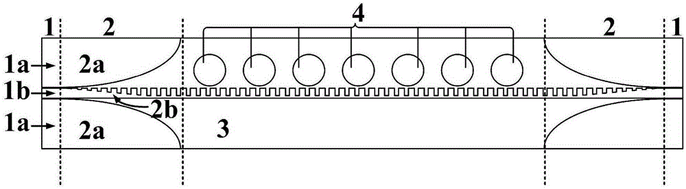
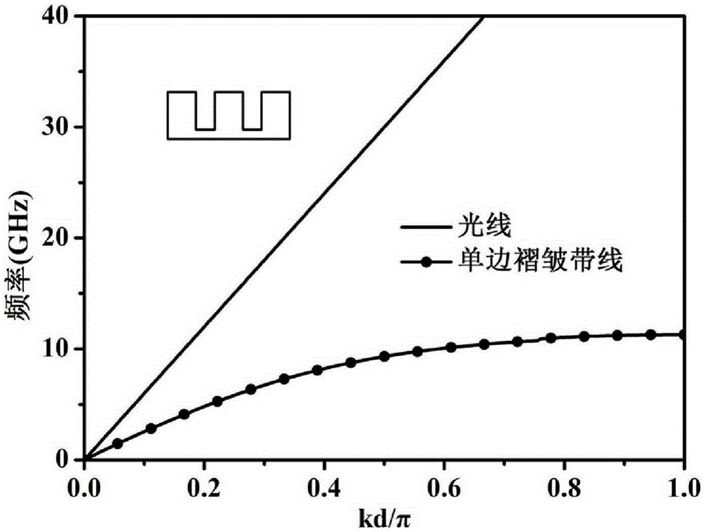
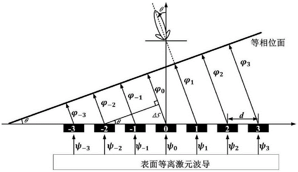
[0029] A wide-angle frequency scanning patch array fed by planar surface plasmons of the present invention adopts the traditional coplanar waveguide transmission line feeding method, and uses planar surface plasmon waveguides to feed metal circular patch arrays. The phase difference of different patch units caused by electricity will cause the change of the scanning angle of the radiation beam. The traditional coplanar waveguide transmission line impedance design is matched to 50 ohms for maximum power transfer; the planar surface plasmon-fed wide-angle frequency-sweeping patch array is from the traditional coplanar waveguide transmission line to the surface plasmon waveguide The transition adopts a unilateral corrugated stripline structure with gradually changing groove depth and an open metal ground structure to achieve wavenumber matching and impedance matching betw...


PUM

PropertyMeasurementUnit
Groove widthaaaaaaaaaa
Depthaaaaaaaaaa
Radiusaaaaaaaaaa

Abstract

The invention discloses a patch array capable of realizing wide angle frequency scanning by employing planar surface plasmon feed. The metal structure comprises coplanar waveguide transmission line feed parts (1) arranged at the two ends, transition parts (2) from coplanar waveguide transmission lines to surface plasmon waveguides, a surface plasmon waveguide part (3) and a round metal patch array (4), wherein the surface plasmon waveguide part (3) is arranged in the middle, the two transition parts (2) are arranged at the two sides of the surface plasmon waveguide part (3), the two coplanar waveguide transmission line feed parts (1) are arranged at two outer sides of the transition parts (2), and the round metal patch array (4) is arranged on the upper part the surface plasmon waveguide part (3). With the structure disclosed by the invention, wide-angle scanning of a beam from the rear side to the front side in a wideband range can be achieved.

Description

technical field [0001] The invention belongs to the field of novel artificial electromagnetic media and wireless communication system electronic devices, in particular to a wide-angle frequency-scan patch array fed by planar surface plasmons. Background technique [0002] Surface plasmon is an electromagnetic mode caused by the coupling of free electrons and light waves (electromagnetic waves) in metals. It propagates at the interface between metal and medium, and at the same time, it is a surface wave that decays exponentially in the direction perpendicular to the interface. However, when the frequency is reduced to the microwave and terahertz bands, metals no longer support such surface plasmons. In order to realize surface plasmons in the microwave and terahertz bands, an artificial surface plasmon has been proposed. The propagation of artificial surface plasmons is realized by using one-dimensional or two-dimensional subwavelength periodic structures on the metal surfac...

Claims


Application Information

Patent Timeline
IPC IPC(8): H01Q21/00H01Q13/10
Inventor 崔铁军尹佳媛
Owner SOUTHEAST UNIV
Why Eureka
Try Eureka