Back failure positioning method of chip
A failure location, chip technology, applied in the field of semiconductor technology, can solve the problem of not reducing photon loss, and achieve the effect of improving product quality and reliability, improving quality and success rate
- Summary
- Abstract
- Description
- Claims
- Application Information
AI Technical Summary
Problems solved by technology
Method used
Image

Examples
Embodiment Construction
[0022] The present invention will be further described below in conjunction with the accompanying drawings and specific embodiments. Obviously, the described examples are only some examples of the present invention, not all examples. Based on the examples summarized in the present invention, all examples obtained by persons of ordinary skill in the art without making creative efforts belong to the protection scope of the present invention.
[0023] It should be noted that, in the case of no conflict, the examples in the present invention and the features in the examples can be freely combined with each other.
[0024] An example of the present invention will be explained in detail below in conjunction with the accompanying drawings.
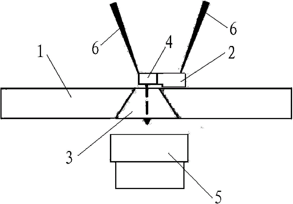
[0025] Such as figure 1 A method for locating a failure on the back of a chip according to an embodiment of the present invention includes the following steps:
[0026] Step 1, providing a light-transmitting thin sheet 1, preferably a glass sli...
PUM
 Abstract
Description
Claims
Application Information