
Wafer transposition system

A technology for wafers and wafers, applied in the field of wafer transposition systems, can solve the problems of reduced wafer performance, high production cost, low transposition efficiency, etc., to reduce the probability of damage and contamination, reduce the probability of damage and contamination, The effect of improving transposition efficiency

Active Publication Date: 2016-02-17
FOUNDER MICROELECTRONICS INT
View PDF4 Cites 1 Cited by
  • Summary
  • Abstract
  • Description
  • Claims
  • Application Information

AI Technical Summary

Problems solved by technology

Not only the transposition efficiency is low, but the production cost is high; it is also easy to cause chip scratches, missing corners, edge chipping, and debris; in addition, the repeated operations of manually transposing the wafers one by one can easily produce particles that contaminate the wafer, resulting in a decrease in the performance of the wafer or scrapping
In particular, the transposition operation of thinned wafers with a thickness of 280 microns is extremely difficult, and the product scrap rate is higher

Method used


Image

  • Wafer transposition system
  • Wafer transposition system
  • Wafer transposition system

Examples


Embodiment Construction

[0053] The following will clearly and completely describe the technical solutions in the embodiments of the present invention with reference to the accompanying drawings in the embodiments of the present invention. Obviously, the described embodiments are only some, not all, embodiments of the present invention. Based on the embodiments of the present invention, all other embodiments obtained by persons of ordinary skill in the art without making creative efforts belong to the protection scope of the present invention.

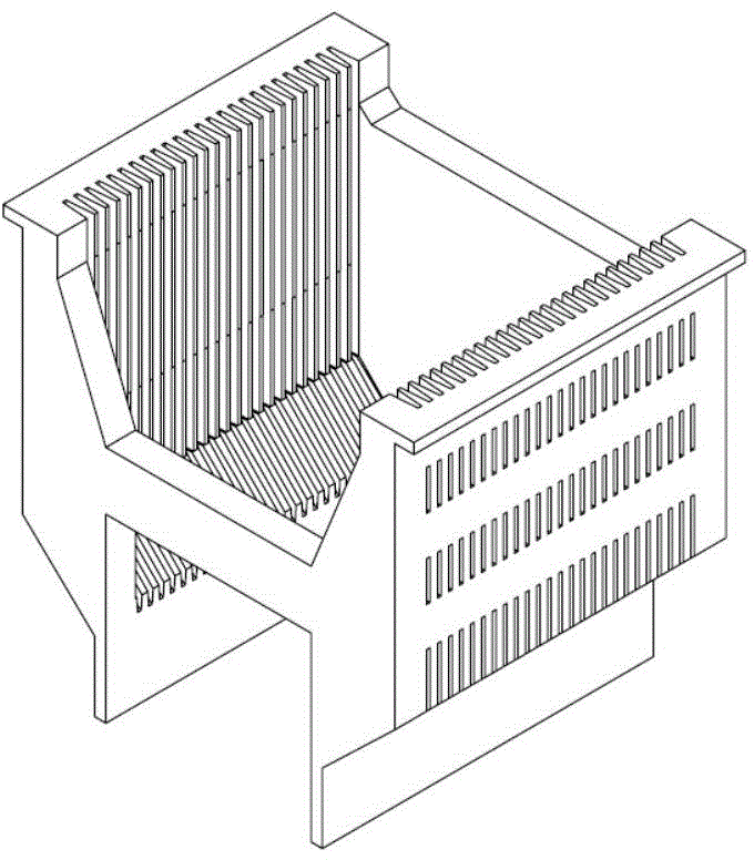
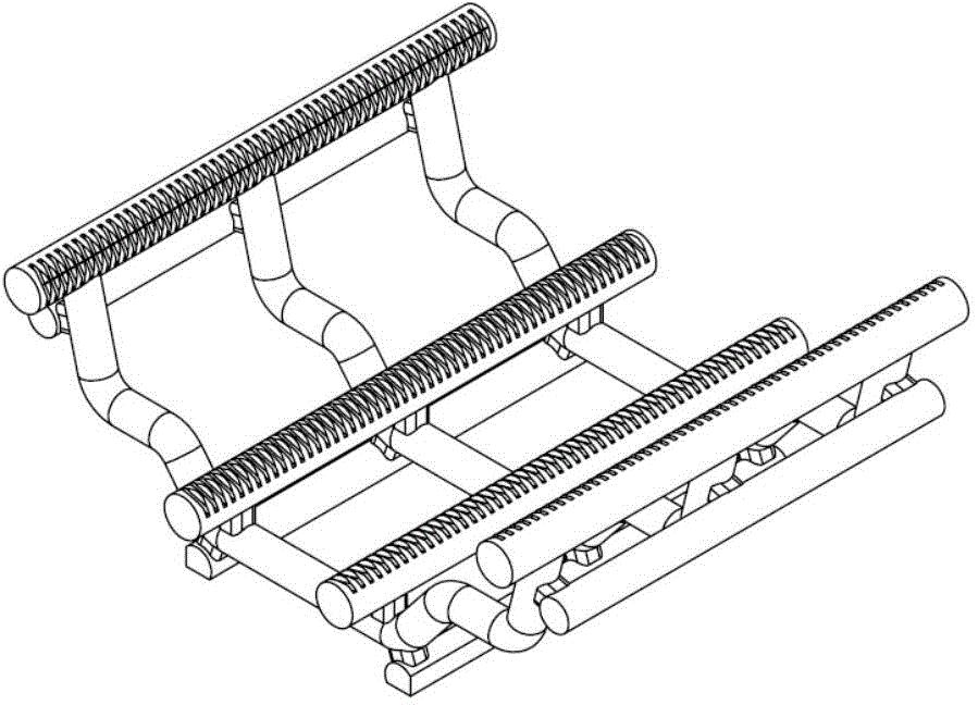
[0054] In the field of semiconductor device production, the wafer used for the production of integrated circuit chips is a single crystal silicon wafer with a diameter of 5 to 12 inches and a thickness between 280-675 microns, such as figure 1 shown. The cassette used for turnover storage has only 25 slots and can only store 25 wafers, such as figure 2 As shown; most of the chip boats used in process production are 50 slots, which can store 50 chips, such as...


PUM


Abstract

The invention discloses a wafer transposition system, for transposing a wafer between a wafer box and a wafer carrying crystal boat. The system comprises a main frame; a turnover apparatus which is used for placing multiple wafers thereon and is fixed to the main frame; and an elevating apparatus which is movably connected with the main frame and cooperates with the turnover apparatus for raising and placing the multiple wafers in the wafer box or the wafer carrying crystal boat in the turnover apparatus and then descending and placing the multiple wafers in the turnover apparatus in the wafer box or the wafer carrying crystal boat. The wafer transposition system, compared to the prior art, improves the transposition efficiency, reduces the probability of damage and pollution caused to the wafers, and reduces the fraction defective of a product.

Description

technical field [0001] The invention relates to the technical field of semiconductor devices, in particular to a wafer transposition system. Background technique [0002] In the field of semiconductor device production, the wafer used for the production of integrated circuit chips is a single crystal silicon wafer with a diameter of 5 to 12 inches and a thickness between 280-675 microns. The production of integrated circuit chips requires many processes and complex processes. According to the process requirements, the wafer will be repeatedly transposed on the process equipment or production fixtures in different processes during the chip production process; especially for the diffusion process, the wafer is transferred from the cassette to the carrier boat, Transpositions to cassettes are extremely heavy and frequent. [0003] Wafer transposition, usually using clip tweezers or vacuum suction pen to manually clamp or absorb one by one from the cassette and then put it int...

Claims


Application Information

Patent Timeline
IPC IPC(8): H01L21/677
Inventor 朱厚华胡德明林伟旺高宏凯
Owner FOUNDER MICROELECTRONICS INT
Learn More