Photoelectric sensor and manufacturing method thereof

A technology of photoelectric sensors and manufacturing methods, applied in the field of semiconductors, capable of solving problems such as high production costs, low resolution, and large thickness

Active Publication Date: 2016-02-17
SHANGHAI OXI TECH
View PDF4 Cites 65 Cited by
  • Summary
  • Abstract
  • Description
  • Claims
  • Application Information

AI Technical Summary

Problems solved by technology

Wherein the first light-shielding layer 02 is on the same metal layer as the gate of the thin film transistor 03, and the drain electrode layer 05 is on the same metal layer as the drain of the thin film transistor 03. It can be seen from the figure that the amorphous silicon photodiode The main part is a stack of P-type layer 08, intermediate layer 07 and N-type layer 06, in which the intermediate layer 07 is lightly doped, so the thickness of the amorphous silicon flat panel detector is approximately above the drain of the thin film transistor 03 The thickness of the laminated layer of the amorphous silicon photodiode is superimposed, and the thickness of the intermediate layer 07 in the amorphous silicon photodiode is about 1 micron, so that the thickness of the amorphous silicon flat panel detector is relatively large, and the incident light is within the range of the flat panel detector.

Method used


Image

  • Photoelectric sensor and manufacturing method thereof
  • Photoelectric sensor and manufacturing method thereof
  • Photoelectric sensor and manufacturing method thereof

Examples


Embodiment Construction

[0104] Existing optical sensors are generally large in size and low in resolution, and are difficult to be used in the field of fingerprint recognition for portable devices.

[0105] In order to solve the above technical problems, the present invention provides a photoelectric sensor and its manufacturing method. The photoelectric sensor has lower production cost and higher resolution, so it can be better applied to fingerprint identification.

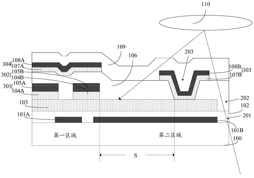
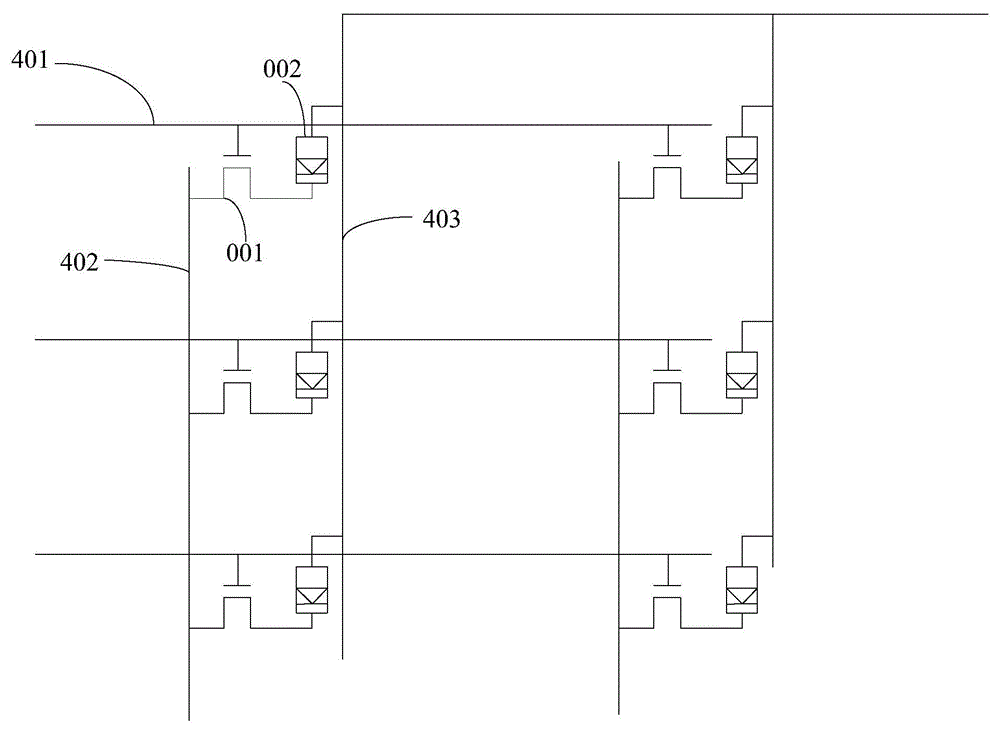
[0106] The present invention firstly provides a photoelectric sensor, which includes a substrate and pixel units on the substrate.

[0107] The technical solution of the photoelectric sensor of the present invention will be described in detail below in conjunction with the accompanying drawings.

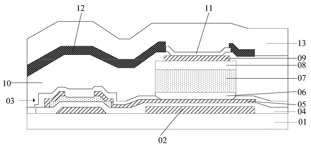
[0108] In this embodiment, the photoelectric sensor is integrated on the array substrate of the LCD panel, that is to say, the photoelectric sensor and the array substrate of the LCD panel have the same manufacturing process, so that the phot...


PUM


Abstract

The invention provides a photoelectric sensor and a manufacturing method thereof. The photoelectric sensor comprises a pixel unit arranged on the substrate; and the pixel unit includes a photodiode and a thin-film transistor. A drain structure of the thin-film transistor servers as a cathode structure of the photodiode, so that the area occupied by the pixel can be reduced and the resolution ratio of the photoelectric sensor can be improved. Moreover, the anode structure and the cathode structure of the photodiode are arranged in a transverse mode, so that the thickness of the photoelectric sensor can be effectively reduced and thus the photoelectric sensor has advantages of small size and high resolution ration. Besides, the manufacturing method of the photoelectric sensor can be combined with the traditional LCD manufacturing method, thereby simplifying the production process of the photoelectric sensor, reducing the production cycle, and effectively reducing the production cost.

Description

technical field [0001] The invention relates to the field of semiconductors, in particular to a photoelectric sensor and a manufacturing method thereof. Background technique [0002] Fingerprint recognition, as a very old biometric method, has recently attracted more attention, especially the prospect of mobile payment has brought broad prospects. People have also invented many methods of fingerprint identification, such as optical, capacitive, microwave, temperature and ultrasonic and many other methods. But each method has its advantages and disadvantages. For example, the traditional optical sensor method cannot be thin and light, especially under the requirement of high resolution. Traditional devices are bulky and cannot be portable, so it is difficult to integrate them into devices such as mobile phones. Although other methods solve the problem of lightness and thinness, they cannot realize large-area arrays, or cannot combine other functions, and the process is comp...

Claims


Application Information

Patent Timeline
IPC IPC(8): H01L27/146
Inventor 林崴平
Owner SHANGHAI OXI TECH
Why Eureka
Try Eureka