System and method for sealing glass packaging body through laser scanning

A technology of laser scanning and sealing glass, which is used in the manufacture of electric solid-state devices, semiconductor devices, and semiconductor/solid-state devices.

Active Publication Date: 2016-02-17
SHANGHAI MICRO ELECTRONICS EQUIP (GRP) CO LTD
View PDF9 Cites 17 Cited by
  • Summary
  • Abstract
  • Description
  • Claims
  • Application Information

AI Technical Summary

Problems solved by technology

[0009] The object of the present invention is to provide a system and method for laser scanning and sealing glass packages, which are used to seal OLED displays or glass packages, which can solve the problem of uneven temperature field distribution of the glass frit, and meanwhile, it has a wider Process window, conducive to improving OLED display yield

Method used


Image

  • System and method for sealing glass packaging body through laser scanning
  • System and method for sealing glass packaging body through laser scanning
  • System and method for sealing glass packaging body through laser scanning

Examples


Embodiment 1

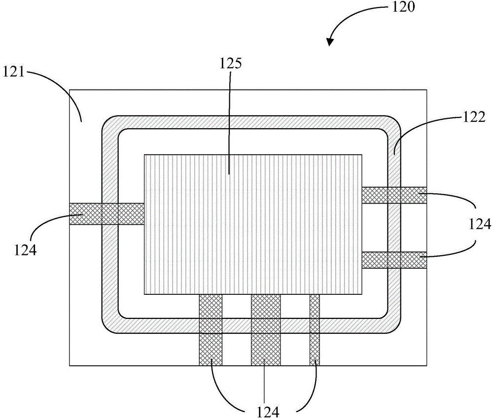
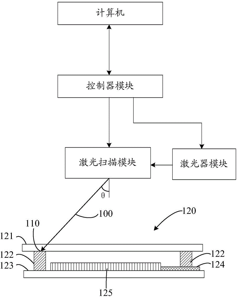
[0051] Please refer to figure 2 and image 3 , in this embodiment, a laser scanning sealing glass package system is proposed, which is used to form a hermetic seal on the OLED display 120 using glass frit, wherein the OLED display 120 is a typical glass package, and the OLED The main structure of the display 120 includes a cover glass 121 , a glass frit 122 , a substrate glass 123 , an OLED layer 125 and an electrode 124 . Wherein, the glass frit 122 is located on the substrate glass 123 of the OLED display 120, and its cross-sectional view is shown in image 3 As shown in the top view as figure 2 shown. The glass frit 122 is pre-cured on the substrate glass 123 through screen printing and pre-sintering steps to form a rounded rectangular sealing line with a certain thickness. The OLED layer 125 on the substrate glass 123 is located inside the sealing line of the glass frit 122 , and there are electrodes 124 on the substrate glass 123 connecting the inside and outside of...

Embodiment 2

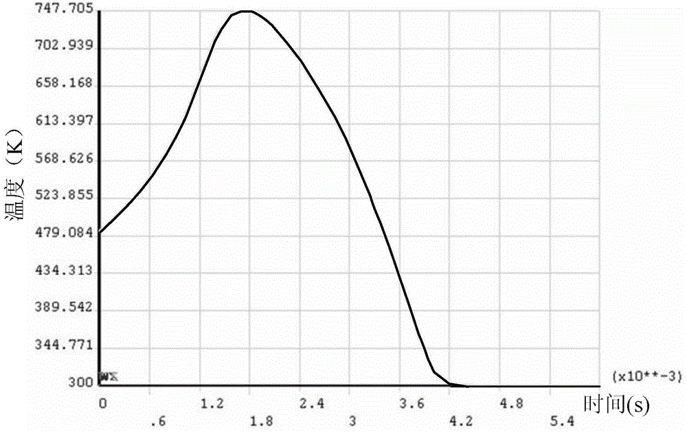
[0067] Please refer to Figure 8 , in this embodiment, the proposed laser scanning sealing glass package system has more temperature measurement modules than in Embodiment 1, and the temperature measurement module is connected to the controller module for measuring the laser irradiation to the glass frit. The real-time temperature of the light spot on the surface is fed back to the controller module. The temperature measurement module can measure the temperature of the glass frit 122 at the position of the light spot 110 in a non-contact and real-time manner, and feed it back to the controller module. One feature is that when the light spot 110 moves at a high speed, the temperature measurement The module can still have sufficient temporal / spatial resolution to measure the temperature of the frit 122 where the spot 110 is located. The controller module can collect and process the temperature signal fed back by the temperature measurement module, and form a closed-loop control...


PUM


Abstract

The invention provides a system and a method for sealing a glass packaging body through laser scanning. A laser scanning module can enable laser to rapidly and periodically scan on glass frit so as to more uniformly heat the glass frit in a synchronous manner, and to solve the problem of uneven temperature field distribution in a packaging process in the prior art; according to the method for sealing the glass packaging body through laser scanning, a laser module can give out laser with a predetermined power curve, so that the heating process of the glass frit can be controlled according to the predetermined power curve; and further more, an additional temperature measurement module can measure and give feedback on real-time temperature on the surface of the glass frit, so that the glass frit can be heated or cooled based on the predetermined heating or cooling curves by adopting predetermined heating or cooling modes and the like.

Description

technical field [0001] The invention relates to the field of optoelectronic semiconductors, in particular to a system and method for laser scanning and sealing a glass package. Background technique [0002] Optoelectronic semiconductor devices have been widely used in various fields of life. Among them, OLED (Organic Light Emitting Diode) has become a research hotspot due to its good color ratio, wide viewing angle, and high response speed, and has a good application prospect. However, the electrodes and organic layers in OLED displays are very sensitive to oxygen and moisture. Oxygen and moisture permeating into the OLED device from the external environment will seriously shorten the life of the OLED device. Therefore, it is very important to provide an effective hermetic seal for OLED devices. Some of the factors that make proper sealing of OLED devices difficult are discussed below: [0003] The hermetic seal shall provide protection against oxygen (10 -3 cm 3 / m2 / d...

Claims


Application Information

Patent Timeline
Patent Type & Authority Applications(China)
IPC IPC(8): H01L51/56
CPCH10K71/00H10K50/84
Inventor 黄元昊朱树存罗闻程蕾丽
Owner SHANGHAI MICRO ELECTRONICS EQUIP (GRP) CO LTD
Why Eureka
Try Eureka