Method for forming circuit board without location holes

A molding method and circuit board technology, which is applied in the direction of printed circuit, printed circuit manufacturing, electrical components, etc., can solve problems such as uneven board edge, too small diameter of through hole, and influence on circuit board splicing, so as to reduce production time, Optimize the production process, facilitate positioning and test the effect

Active Publication Date: 2016-02-17
VICTORY GIANT TECH HUIZHOU CO LTD
View PDF4 Cites 24 Cited by
  • Summary
  • Abstract
  • Description
  • Claims
  • Application Information

AI Technical Summary

Problems solved by technology

[0002] With the continuous development of the circuit board industry, circuit boards for various purposes also appear, and the production requirements are becoming more and more sophisticated and refined, especially because the backplane of the large-scale LED display is spliced ​​​​by multiple circuit boards. There is no positioning through hole or the diameter of the through hole is too small (below 1.0MM). The seamless splicing between the circuit boards is the key to the LED display effect. The traditional operation method can no longer meet this requirement. As a circuit board manufacturer, research and development of new The production method reduces the production cost, improves the production efficiency, and manufactures the circuit board that meets the customer's requirements is the direction of the circuit board manufacturer's efforts. At the same time, the management of the production process has become the key to the production of high-quality products.
[0003] In the circuit board design stage, if there is no positioning hole in the board or the diameter of the through hole is too small (below 1.0mm), the usual practice is to add a process edge in the design, and add a positioning hole that meets the requirements on the process edge to facilitate forming processing. The process edge will be removed after the parts are pasted. Therefore, there are two common ways to remove the process edge: 1. Design stamp holes to connect the main body of the circuit board with the process edge. After the parts are attached, remove the process edge (see attached figure 1 ); 2. Design the main body of the circuit board to be directly connected to the process edge, cut the V groove through V-CUT, and remove the process edge after the attachment is completed (see attached figure 2 ); but the above two designs for removing the process edge are limited to customers who allow the process edge to be shipped, and the board edge is not smooth after the process edge is removed, which directly affects the splicing between the circuit boards. If the customer does not allow the process edge to be added, Neither of the above two designs can be used

Method used


Image

  • Method for forming circuit board without location holes
  • Method for forming circuit board without location holes
  • Method for forming circuit board without location holes

Examples


Embodiment Construction

[0027] In order to allow those skilled in the art to better understand the technical solutions of the present invention, the present invention will be further described below in conjunction with the accompanying drawings.

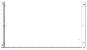
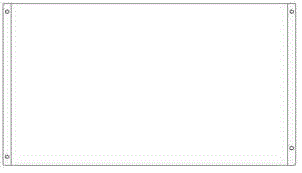
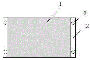
[0028] Such as Figure 3 to Figure 8 As shown, a circuit board molding method without positioning holes includes a circuit board 1 to be processed that is provided with two process sides 2, such as image 3 As shown; the two process sides 2 of the circuit board to be processed are arranged on any two sides of the circuit board to be processed. Wherein each process edge 2 is provided with two positioning holes 3, and the circuit board to be processed is positioned through the positioning holes. Specific steps are as follows:

[0029] S1. Put multiple circuit boards to be processed to the outside in sequence, and then overlap and fix them on the backing plate of the forming machine table; then put the circuit board 1 to be processed into the gong board equi...


PUM


Abstract

The invention discloses a method for forming a circuit board without location holes. A circuit board to be processed with two technological edge is included, and each technological edge is provided with two location holes. The method comprises the following concrete steps: S1, carrying out a primary milling formation to prepare semi-finished product circuit boards A; S2, carrying out an electric test; S3, successively aligning the semi-finished product circuit boards A and overlapping the semi-finished product circuit boards A on the bench surface of a formation machine, one technological edge of the multiple semi-finished product circuit boards A is fixed by use of a positioning pin, and boring is performed at board edge positions of the multiple semi-finished product circuit boards A, and the semi-finished product circuit boards A are fixed by use of positioning pins; S4, carrying out secondary milling to prepare semi-finished product circuit boards B; S5, boring is performed at positions, close to board edges, of the semi-finished product circuit boards B after the technological edges are milled, and the semi-finished product circuit boards B are fixed by use of the positioning pins; S6, carrying out third-time milling to prepare a finished product circuit board; and S7, cleaning, and performing drying processing. According to the invention, milling formation is used for three times, a circuit board formation method is optimized, the board edge of the circuit board is enabled to be flat and smooth, splicing application is facilitated, the quality of the circuit board is improved, the production time is reduced, and the production efficiency is improved.

Description

technical field [0001] The invention belongs to the technical field of circuit board production, and in particular relates to a method for forming a circuit board without positioning holes. Background technique [0002] With the continuous development of the circuit board industry, circuit boards for various purposes also appear, and the production requirements are becoming more and more sophisticated and refined, especially because the backplane of the large-scale LED display is spliced ​​​​by multiple circuit boards. There is no positioning through hole or the diameter of the through hole is too small (below 1.0MM). The seamless splicing between the circuit boards is the key to the LED display effect. The traditional operation method can no longer meet this requirement. As a circuit board manufacturer, research and development of new It is the direction of circuit board manufacturers to reduce production costs, improve production efficiency, and produce circuit boards that...

Claims


Application Information

Patent Timeline
Patent Type & Authority Applications(China)
IPC IPC(8): H05K3/00
CPCH05K3/0044H05K2203/1476
Inventor 李雄杰王忱樊建华黄慧
Owner VICTORY GIANT TECH HUIZHOU CO LTD
Why Eureka
Try Eureka