Method and apparatus for creating perfect microwave absorbing printed circuit boards

A printed circuit board, gravure printing technology, applied in the direction of printed circuits, circuit devices, printed circuits, etc., can solve problems such as influence

Inactive Publication Date: 2016-02-17
FLEXTRONICS AP LLC
View PDF5 Cites 9 Cited by
  • Summary
  • Abstract
  • Description
  • Claims
  • Application Information

AI Technical Summary

Problems solved by technology

This trapped energy may adversely affect other components on the board and may inhibit the board from operating properly
Aside from the constraints rela

Method used


Image

  • Method and apparatus for creating perfect microwave absorbing printed circuit boards
  • Method and apparatus for creating perfect microwave absorbing printed circuit boards
  • Method and apparatus for creating perfect microwave absorbing printed circuit boards

Examples


Embodiment Construction

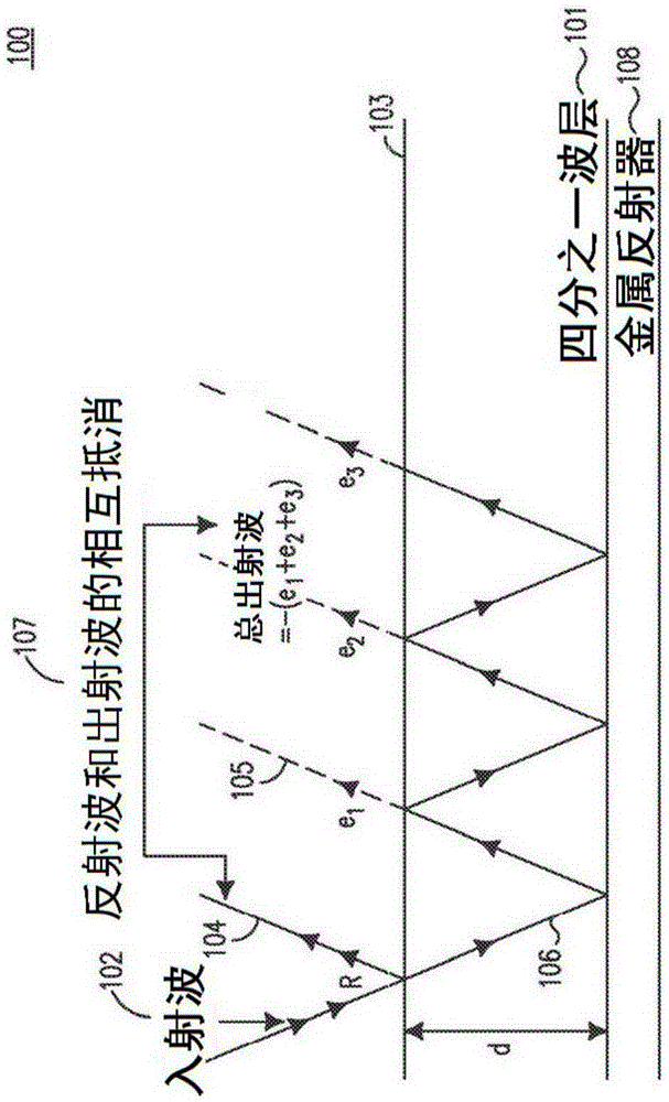
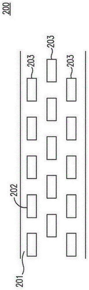
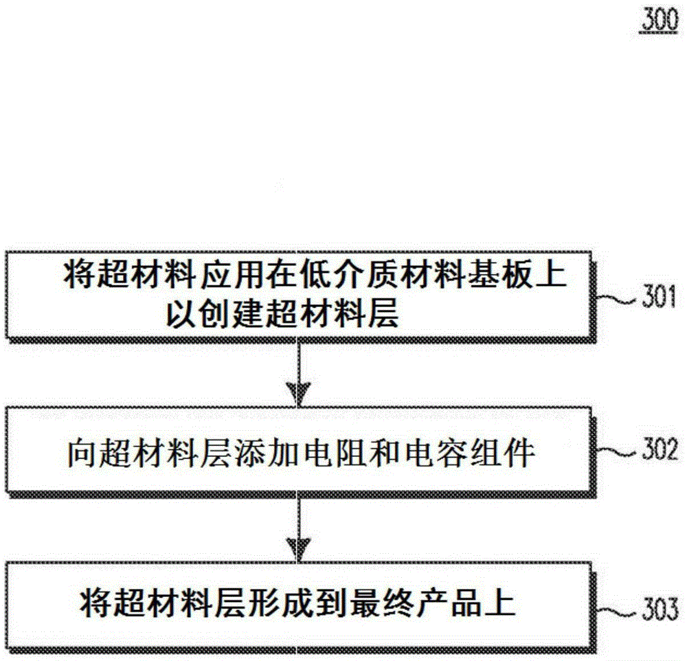
[0017] In this paper is described a concept for exploiting the unique properties of fabricated metamaterials (as absorbers) to produce radio frequency absorber (RFA) or fully microwave absorber (PMA) printed circuit boards (PCBs) by applying to layers in PCBs methods and devices. According to embodiments described herein, a metamaterial layer in a PCB can be used as an RFA or PMA layer.

[0018] Magnetic materials (eg, permalloy, musalloy, etc.) may be transformed into a physical format that will be suitable for use with an appropriate adhesive and for use in any of the embodiments described herein. Typically, magnetic materials can be processed from bulk metal to spheres, rods, or flakes. Magnetic material geometries used in absorbers It can be pointed out that flake geometries have clear advantages over other geometries when constructing successful absorbers. Additionally, the aspect ratio of the material in any geometry may be critical for achieving maximum permittivity a...


PUM


Abstract

A method and apparatus for producing a radio frequency absorbing (RFA) or perfect microwave absorbing (PMA) printed circuit board (PCB) is described herein. A metamaterial layer may be applied to a low dielectric substrate. Resistive and capacitive components may then be added to the metamaterial layer. The metamaterial layer may then be formed into an RFA or PMA PCB, which may comprise a multi-layered assembly for absorption of electromagnetic radiation in a targeted frequency range such as the microwave frequency range in the PCB.

Description

[0001] Cross References to Related Applications [0002] This application claims the benefit of US Provisional Application Serial No. 61 / 791,098 filed March 15, 2013, the contents of which are hereby incorporated by reference. Background technique [0003] As technology continues to improve and more and more electronic devices become more common in all industries, the concern for electromagnetic interference (EMI) has become extremely important. Electromagnetic interference, also known as radio frequency interference (RFI), is a disturbance that can affect an electronic circuit due to electromagnetic induction or radiation emitted from an external source. External sources can be man-made or natural, making it extremely difficult to address due to the large variety in where EMI can originate. Devices such as cellular phones, tablets, and computers are some of the main emitters of EMI. Electronic instruments such as these can eventually cause destruction, degradation, or inter...

Claims


Application Information

Patent Timeline
IPC IPC(8): H01Q17/00H05K1/02
CPCH01Q17/002H05K1/0236H05K1/024H05K1/0233H05K2201/083G02B2207/121Y10T156/1002Y10T29/49018H05K9/0088H01Q17/00
Inventor P·索尔萨
Owner FLEXTRONICS AP LLC
Why Eureka
Try Eureka