Alignment method for photolithography process

A lithography process and pre-alignment technology, applied in the field of lithography process, can solve the problems of inability to complete the lithography process, penetration, and alignment failure, etc., and achieve the effect of solving strong light absorption and exposure alignment failure

Active Publication Date: 2018-09-21
WUHAN XINXIN SEMICON MFG CO LTD
View PDF4 Cites 0 Cited by
  • Summary
  • Abstract
  • Description
  • Claims
  • Application Information

AI Technical Summary

Problems solved by technology

However, this kind of film layer has strong light absorption. When photolithography is used to align the front layer, the light basically cannot penetrate this layer of film, resulting in the reception of the alignment mark light signal without the front layer, resulting in alignment failure and failure. Complete the subsequent photolithography process

Method used


Image

  • Alignment method for photolithography process
  • Alignment method for photolithography process

Examples


Embodiment Construction

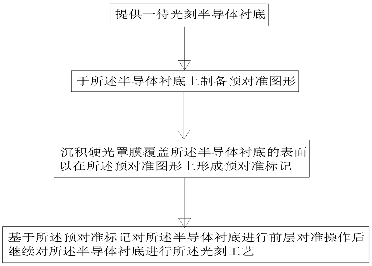
[0020] Such as figure 1 As shown, a kind of lithography process alignment method of the present invention mainly comprises the following steps: provide a semiconductor substrate to be photoetched and prepare pre-alignment pattern on this semiconductor substrate; Deposit hard mask film (preferably Kodiak film) to cover the surface of the semiconductor substrate to form a pre-alignment mark on the pre-alignment pattern; then, after performing the front layer alignment operation on the semiconductor substrate based on the pre-alignment mark, continue the semiconductor substrate performing the photolithography process; wherein, the hard mask film has a light absorption property.

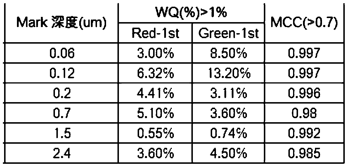
[0021] As a preferred embodiment, the above-mentioned pre-alignment pattern includes several strip parallel grooves, the depth of which is less than 120nm.

[0022] As a preferred embodiment, when the front-layer alignment operation is performed, the alignment light utilizes the undulating topography fo...


PUM

PropertyMeasurementUnit
depthaaaaaaaaaa

Abstract

The present invention relates to the technical field of photolithography technology, and in particular to a photolithography process alignment method, which provides a semiconductor substrate to be photoetched, before depositing a high light-absorbing film on the surface of the semiconductor substrate to form a pre-alignment mark. A new alignment mask is etched on the surface of the semiconductor substrate to form a pre-alignment pattern, and then the front-layer alignment operation is performed on the semiconductor substrate based on the pre-alignment marks, and the pre-alignment marks are deposited and formed The topography of the mask is used for alignment, and the alignment light does not need to penetrate the high light-absorbing film layer, avoiding a large amount of light absorption to achieve exposure alignment.

Description

technical field [0001] The present invention relates to the technical field of photolithography technology, in particular to a photolithography process alignment method. Background technique [0002] Some layers in the 3D process technology need to use ultra-deep hole etching, and ultra-deep hole etching requires a good conformal material as a hard mask (Hard Mask) to transfer the pattern to the substrate. The industry now commonly uses Kodiak film as a hard mask (HM) to transfer graphics. However, this kind of film layer has strong light absorption. When photolithography is used to align the front layer, the light basically cannot penetrate this layer of film, resulting in the reception of the alignment mark light signal without the front layer, resulting in alignment failure and failure. Complete the subsequent photolithography process. Contents of the invention [0003] In view of the above problems, the present invention provides a photolithography process alignment ...

Claims


Application Information

Patent Timeline
Patent Type & Authority Patents(China)
IPC IPC(8): G03F9/00G03F1/42
CPCG03F1/42G03F9/00
Inventor 万浩陈保友许刚盛二威王猛
Owner WUHAN XINXIN SEMICON MFG CO LTD
Why Eureka
Try Eureka