Qualifying patterns, patterning processes, or patterning apparatus in the fabrication of microlithographic patterns

a technology of microlithography and process, applied in the field of manufacturing microelectronic devices, can solve the problems of affecting yield, affecting yield, and difficult to manufacture resistive devices, and achieve the effect of reducing depth of focus, amplifying any unexpected patterning behavior, and maximizing the available process window

Active Publication Date: 2008-08-26
KLA TENCOR TECH CORP
View PDF17 Cites 106 Cited by
  • Summary
  • Abstract
  • Description
  • Claims
  • Application Information

AI Technical Summary

Benefits of technology

[0010]A preferred implementation is a method of qualifying incoming reticles and process conditions on test wafers to maximize the available usable process window for a given reticle exposure tool combination. The method qualifies the image produced by the cumulative effect of various configurations of illumination sources, optical proximity correction artifacts, phase shifted imaging, and various photochemical processing techniques implemented at the imaging plane. Practicing this method on test wafers enables the identification of spatial areas where a process will fail first and candidate regions for carrying out defect inspection and metrology.
[0011]The nature of process window qualification is to induce pattern anomalies, such as transient repeating defects, by varying a process parameter or operating variable. One example o

Problems solved by technology

Although they are implemented in semiconductor device designs to facilitate low k1 lithography, these RET make reticles more difficult and consequently more expensive to manufacture.
Marginal RET designs not noted by simulation checks translate into electrical failures in wafer fabrication, affect yield, and possibly remain unnoticed until wafer fabrication is complet

Method used


Image

  • Qualifying patterns, patterning processes, or patterning apparatus in the fabrication of microlithographic patterns
  • Qualifying patterns, patterning processes, or patterning apparatus in the fabrication of microlithographic patterns
  • Qualifying patterns, patterning processes, or patterning apparatus in the fabrication of microlithographic patterns

Examples


Embodiment Construction

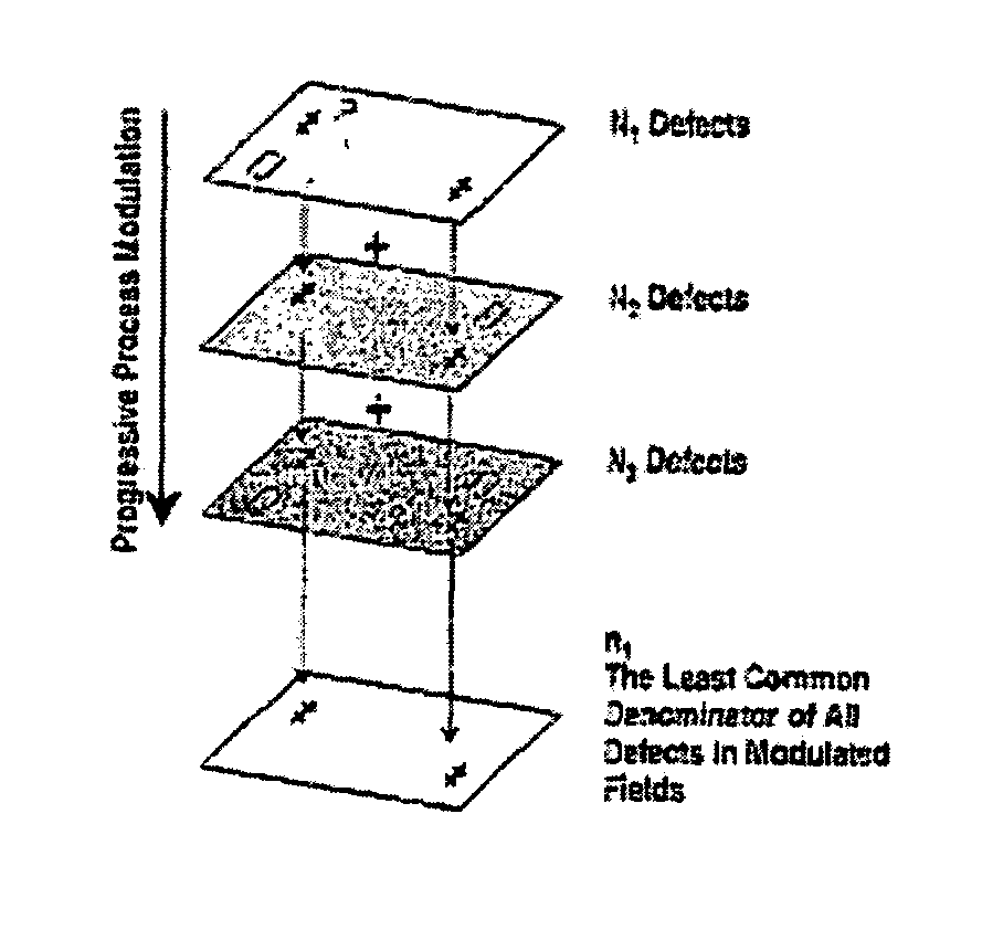
[0040]As used herein, the term “reticle” is used interchangeably with the term “mask.” In addition, the term “defect” is used interchangeably with the term “anomaly.”

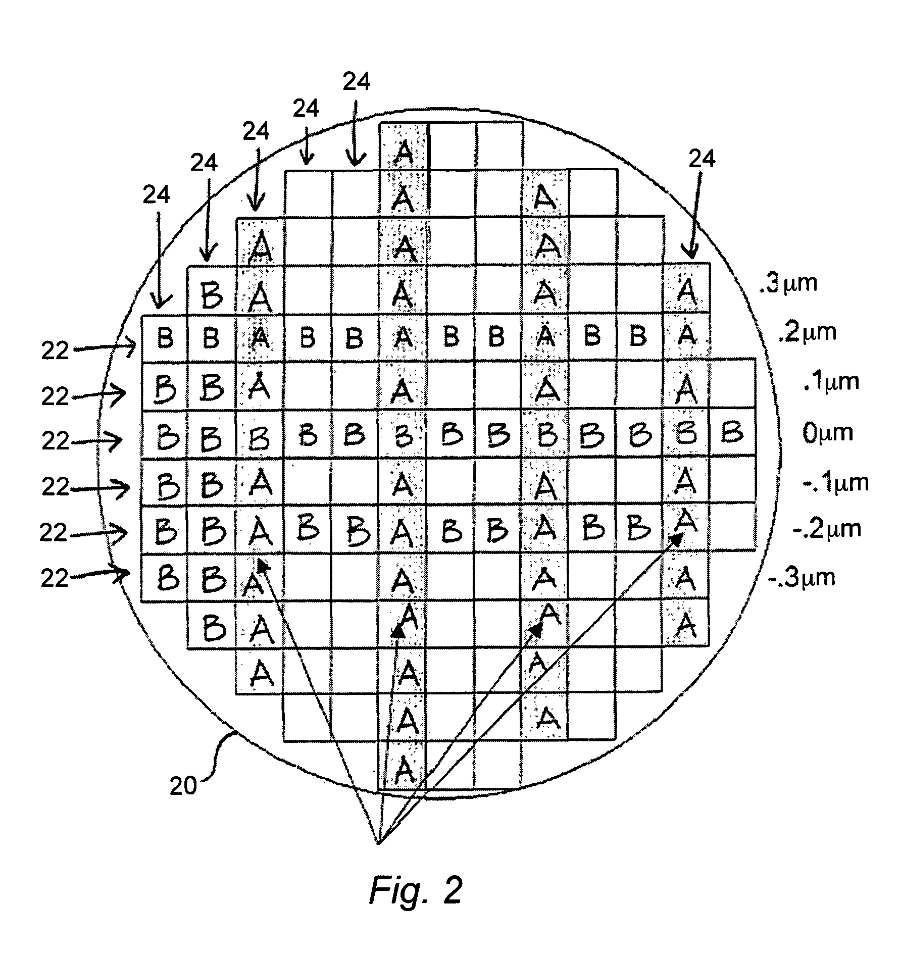
[0041]A preferred embodiment implements modulation of focus of light illuminating reticles, each of which is used to expose by a step and repeat or a step and scan process a top layer of photoresist covering a test wafer. The reticles are printed on optimized film stacks, the type of optimization depending on the type of process level, which includes contact or via, gate, and trench. The base film stack is preferably a simple thermally grown or deposited stack of 1050 Å oxide covered by 320 Å SiON or any other base film stack known in the art.

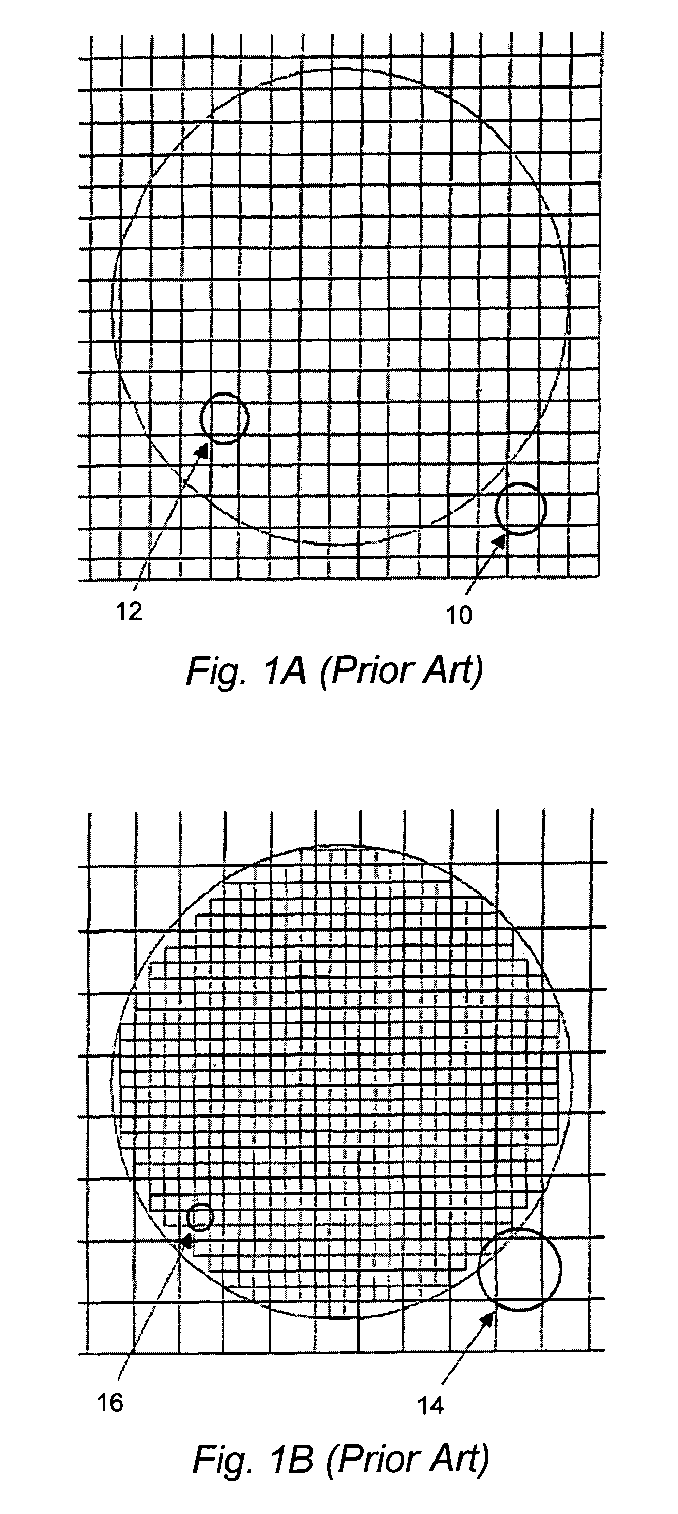
[0042]FIGS. 1A and 1B show, respectively, prior art single die reticle (exposure field 10 contains one unique die 12) and prior art multi-die reticle (array of multiple rows and columns of nominally identical die where exposure field 14 contains multiple die 16) wafer layouts and i...


PUM


Abstract

Methods that include acquiring aerial images of a reticle for different values of a member of a set of lithographic variables are provided. One method also includes determining a presence of an anomaly in a design pattern of the reticle by comparing at least one pair of the aerial images corresponding to at least two of the different values. A different method includes comparing at least one pair of the aerial images corresponding to at least two of the different values and determining an area on the reticle where a lithography process using the reticle is most susceptible to failure based on the results of the comparison. Another embodiment includes determining a presence of transient repeating defects on the reticle by subtracting non-transient defects from the aerial images and comparing at least one pair of the aerial images corresponding to at least two of the different values.

Description

PRIORITY CLAIM[0001]This application claims priority to U.S. Provisional Application No. 60 / 396,197 entitled “Qualifying Patterns, Patterning Processes, or Patterning Apparatus in the Fabrication of Microlithographic Patterns,” filed Jul. 15, 2002, which is incorporated by reference as if fully set forth herein. This application also claims priority to U.S. Provisional Application No. 60 / 485,233 entitled “Qualifying Patterns, Patterning Processes, or Patterning Apparatus in the Fabrication of Microlithographic Patterns,” filed Jul. 7, 2003, which is incorporated by reference as if fully set forth herein.BACKGROUND OF THE INVENTION[0002]1. Field of the Invention[0003]This invention relates to the manufacture of microelectronic devices and, in particular, to a method of qualifying a pattern, patterning process, or patterning apparatus used in the fabrication of microlithographic patterns for producing microelectronic devices.[0004]2. Description of the Related Art[0005]The rapid decre...

Claims


Application Information

Patent Timeline
IPC IPC(8): G06K9/00G02B21/06G06F17/50H04N7/18G03FG03F1/00G03F7/20H01L21/027
CPCG03F1/84G03F7/70666G03F7/7065
Inventor PETERSON, INGRID B.VON DEN HOFF, MIKEWILEY, JIM
Owner KLA TENCOR TECH CORP
Why Eureka
Try Eureka