Connecting method and system for communication between rate configurable FPGA chips

A connection system and connection method technology, applied in FPGA communication and FPGA fields, can solve the problems of long verification period and low verification efficiency, achieve strong versatility and practicability, save costs, and shorten the design verification cycle.

Active Publication Date: 2016-02-24
SHANGHAI ADVANCED RES INST CHINESE ACADEMY OF SCI +1
View PDF3 Cites 13 Cited by
  • Summary
  • Abstract
  • Description
  • Claims
  • Application Information

AI Technical Summary

Problems solved by technology

[0005] In view of the shortcomings of the prior art described above, the purpose of the present invention is to provide a connection method and system for inter-chip communication of a rate configurable FPGA, which is used to solve the problems of long cycle and low verification efficiency in FPGA test verification in the prior art. question

Method used


Image

  • Connecting method and system for communication between rate configurable FPGA chips
  • Connecting method and system for communication between rate configurable FPGA chips
  • Connecting method and system for communication between rate configurable FPGA chips

Examples


Embodiment Construction

[0035] Embodiments of the present invention are described below through specific examples, and those skilled in the art can easily understand other advantages and effects of the present invention from the content disclosed in this specification. The present invention can also be implemented or applied through other different specific implementation modes, and various modifications or changes can be made to the details in this specification based on different viewpoints and applications without departing from the spirit of the present invention.

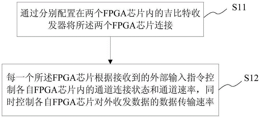
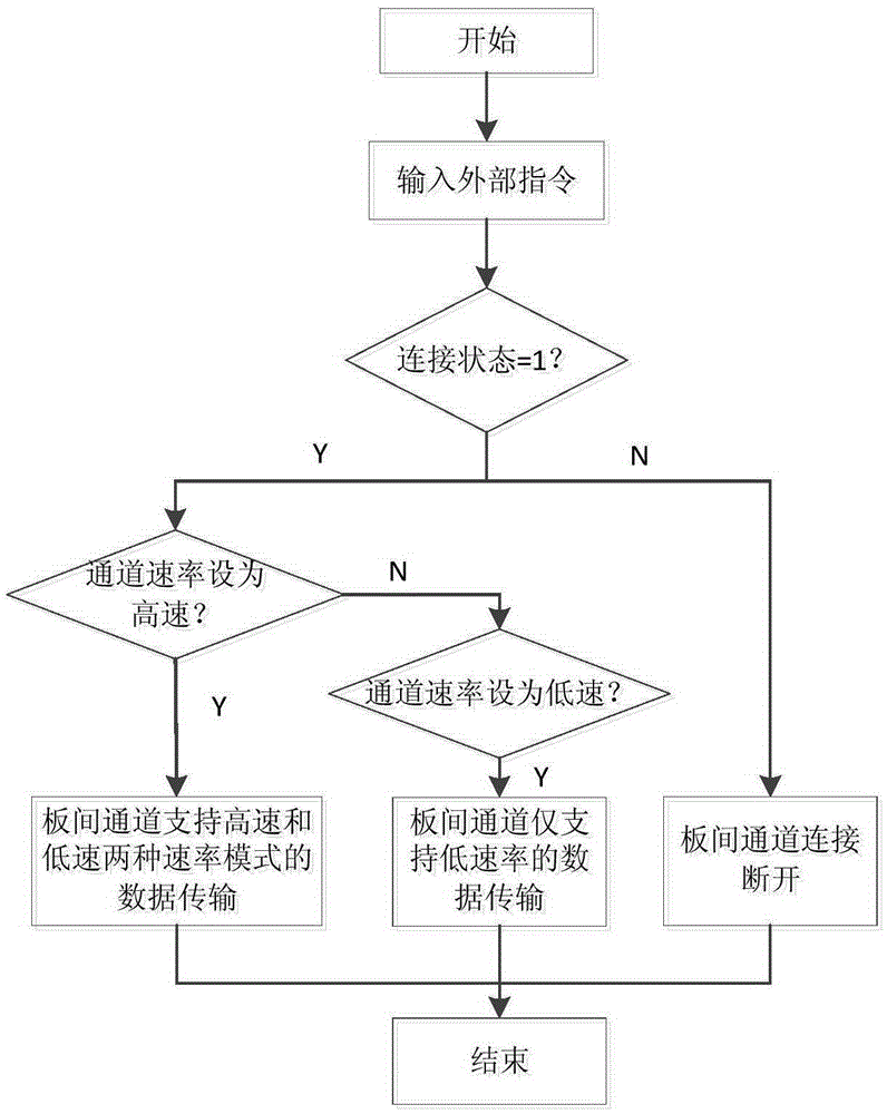
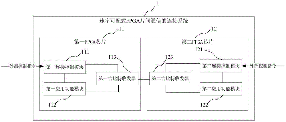
[0036] The purpose of this embodiment is to provide a rate-configurable FPGA inter-chip communication connection method and system, which are used to solve the problems of long FPGA testing and verification period and low verification efficiency in the prior art. The principle and implementation of a connection method and system for rate-configurable FPGA inter-chip communication of this embodiment will be described in detail below, so...


PUM


Abstract

The present invention provides a connecting method and system for communication between rate configurable FPGA chips. The method comprises: connecting two FPGA chips through Gigabit transceivers respectively configured in the two FPGA chips. Each of the FPGA chips is configured with a connection state write register and a channel rate write register, which are respectively used for controlling channel connection states and channel rates in respective FPGA chips according to received external input instructions, while controlling the matching with data transmission rates of the respective FPGA chips receiving and transmitting data, thereby finally realizing switching control of inter-board data links. According to the connecting method and system, high and low-rate data transmission modes are compatible, and different rate modes are independent of each other and non-interfering; and a design verification mode compatible with high and low rates can set up a plurality of test environments at the same time to perform verification, cause no influence on transmission performance for change of a rate mode, effectively shorten a design verification period and reduce costs.

Description

technical field [0001] The invention relates to the field of FPGA technology, in particular to the field of FPGA communication technology, in particular to a connection method and system for rate-configurable FPGA interchip communication. Background technique [0002] With the development of large-scale integrated circuits, the data transmission rate is also increasing. The parallel I / O interface represented by the traditional PCI bus technology can no longer meet the needs of the network and user terminals for the communication bandwidth of the high-speed I / O interface. Serial communication technology becomes mainstream. [0003] The serial communication technology represented by Serdes reduces the number of required channels and device pins, and the single-channel communication capability can reach 28Gbps. This technology puts forward higher requirements for the board-level verification scheme in the chip design process. One verification scheme is to connect the high-spee...

Claims


Application Information

Patent Timeline
Patent Type & Authority Applications(China)
IPC IPC(8): G06F13/40
CPCG06F13/4068G06F2213/0016G06F2213/0038
Inventor 王鹏吴涛高鹏
Owner SHANGHAI ADVANCED RES INST CHINESE ACADEMY OF SCI
Why Eureka
Try Eureka