A light-trapping structure, its manufacturing method, and a thin-film solar cell using the structure

A light trapping structure and interference light technology, applied in photovoltaic power generation, circuits, electrical components, etc., can solve the problems of complex manufacturing process, limited increase in spectral absorption range, cluttered and disordered structure, etc., and achieve good angle sensitivity, simple and fast. The effect of making, strong coupling characteristics

Inactive Publication Date: 2017-11-24
UNIV OF ELECTRONICS SCI & TECH OF CHINA
View PDF3 Cites 0 Cited by
  • Summary
  • Abstract
  • Description
  • Claims
  • Application Information

AI Technical Summary

Problems solved by technology

However, the preparation method of wet etching often also forms disordered structures
Although random and disordered light-trapping structures can obtain absorption growth in a wide spectral range, it is difficult to achieve maximum enhanced absorption due to structural disorder.
In order to arrange the nanostructures in an orderly manner, they used a combination of mask photolithography and wet etching, but this method is only applicable to single crystal silicon solar cells
[0004] On the whole, the range of spectral absorption that can be achieved by using disordered structures or pyramids in existing technologies is limited, the absorption efficiency is not high, the manufacturing process is complicated, and the cost is also high

Method used


Image

  • A light-trapping structure, its manufacturing method, and a thin-film solar cell using the structure
  • A light-trapping structure, its manufacturing method, and a thin-film solar cell using the structure
  • A light-trapping structure, its manufacturing method, and a thin-film solar cell using the structure

Examples


Embodiment Construction

[0021] In order to make the object, technical solution and advantages of the present invention clearer, the present invention will be further described in detail below in conjunction with the accompanying drawings and embodiments. It should be understood that the specific embodiments described here are only used to explain the present invention, not to limit the present invention.

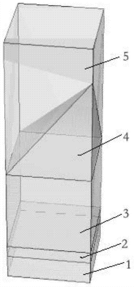
[0022] figure 1 An embodiment of a light-trapping structure of the present invention is shown: a light-trapping structure comprising a two-dimensional right-angled quadrangular pyramid-shaped light-trapping silicon layer 4, and the two-dimensional right-angled square-pyramid-shaped light-trapping silicon layer 4 is made of micro-nano Periodic and non-completely symmetrical two-dimensional right-angled quadrangular pyramid arrays, wherein the shape of a single periodic two-dimensional right-angled quadrangular pyramid is: the bottom is a square, one edge is perpendicular to the bottom, and the two s...


PUM


Abstract

The invention relates to a light trapping structure, a method for making the same, and a thin-film solar cell using the structure. The light trapping structure comprises a two-dimensional right-angled quadrangular pyramid light trapping silicon layer (4), the two-dimensional right-angled quadrangular pyramid trapping light The silicon layer (4) is composed of a micro-nano periodic and non-completely symmetrical two-dimensional right-angled quadrangular pyramid array, wherein the shape of a single periodic two-dimensional right-angled quadrangular pyramid is: the bottom surface is a square, an edge is perpendicular to the bottom surface, and the edge is perpendicular to the bottom surface. The two side surfaces adjacent to the sides are perpendicular to the bottom surface, and the other two side surfaces are inclined to the bottom surface. The light trapping structure disclosed by the invention has strong coupling characteristics, has the characteristics of wide spectrum absorption enhancement and good angle sensitivity, and the absorption enhancement effect is better than that of the traditional inverted pyramid and other structures.

Description

technical field [0001] The invention relates to a light-trapping structure, a manufacturing method thereof and a thin-film solar cell using the structure. Background technique [0002] In recent years, with the progress of science and technology and the development of economy, the demand for energy in various countries is increasing, and non-renewable energy sources such as electricity, coal, and oil are frequently in urgent need, which promotes the rapid development of the photovoltaic industry. The core device of solar photovoltaic power generation is solar cells. Silicon solar cells occupy a dominant position in solar cells due to their wide range of sources and low cost. At present, solar cells mainly include crystalline silicon solar cells and thin film solar cells. Compared with crystalline silicon solar cells, thin-film solar cells have the advantages of low cost, large-area production, and better low-light performance. However, since the thickness of the absorbing ...

Claims


Application Information

Patent Timeline
Patent Type & Authority Patents(China)
IPC IPC(8): H01L31/054H01L31/0445
CPCY02E10/52
Inventor 郭小伟周勇柳邦
Owner UNIV OF ELECTRONICS SCI & TECH OF CHINA
Why Eureka
Try Eureka