Two-dimensional cosine wave surface light-trapping structure and solar thin film battery based on this structure

A technology of solar cells and light trapping structures, applied in photovoltaic power generation, circuits, electrical components, etc., can solve the problems of disordered structure, area limitation, inability to prepare nanostructures, etc., and achieve good angle sensitivity, strong coupling characteristics, The effect of large forming area

Inactive Publication Date: 2017-03-01
UNIV OF ELECTRONICS SCI & TECH OF CHINA
View PDF5 Cites 0 Cited by
  • Summary
  • Abstract
  • Description
  • Claims
  • Application Information

AI Technical Summary

Problems solved by technology

However, the preparation method of self-assembly is usually limited by the area, and it is impossible to prepare large-area ordered nanostructures.
In 2013, M.Foldyna et al. can also prepare nanowire structures through the gas-liquid-solid growth mechanism, but the nanoarrays formed by this method are mostly disordered
However, the preparation method of wet etching often also forms disordered structures
Although random and disordered light-trapping structures can obtain absorption growth in a wide spectral range, it is difficult to achieve maximum enhanced absorption due to structural disorder.
In order to arrange the nanostructures in an orderly manner, they used a combination of mask photolithography and wet etching, but this method is only applicable to single crystal silicon solar cells

Method used


Image

  • Two-dimensional cosine wave surface light-trapping structure and solar thin film battery based on this structure
  • Two-dimensional cosine wave surface light-trapping structure and solar thin film battery based on this structure
  • Two-dimensional cosine wave surface light-trapping structure and solar thin film battery based on this structure

Examples


preparation example Construction

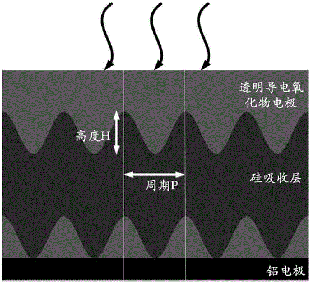
[0022] The method for preparing a silicon-based thin-film solar cell in the present invention includes the following steps: depositing a transparent conductive oxide on the metal electrode substrate, using interference photolithography to make a cosine wave light trapping structure, and then sequentially depositing and doping to make a silicon absorber Layer PN junction, and then use interference lithography to make a cosine waveform light trapping structure, and finally deposit a transparent conductive oxide.

[0023] The absorption enhancement effect of the periodic two-dimensional cosine wave surface light trapping structure can be based on the short-circuit current density at normal incidence J sc To evaluate, its expression is as follows:

[0024]

[0025] Where q is the amount of charge, λ is the wavelength of incident light, h is Planck's constant, c is the speed of light, I AM1.5G (λ) is the AM1.5G solar spectrum radiation, and A(λ) is the absorption spectrum of the batte...

Embodiment 1

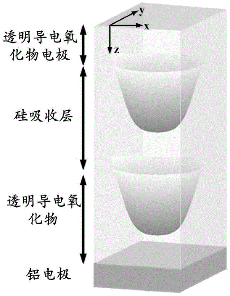
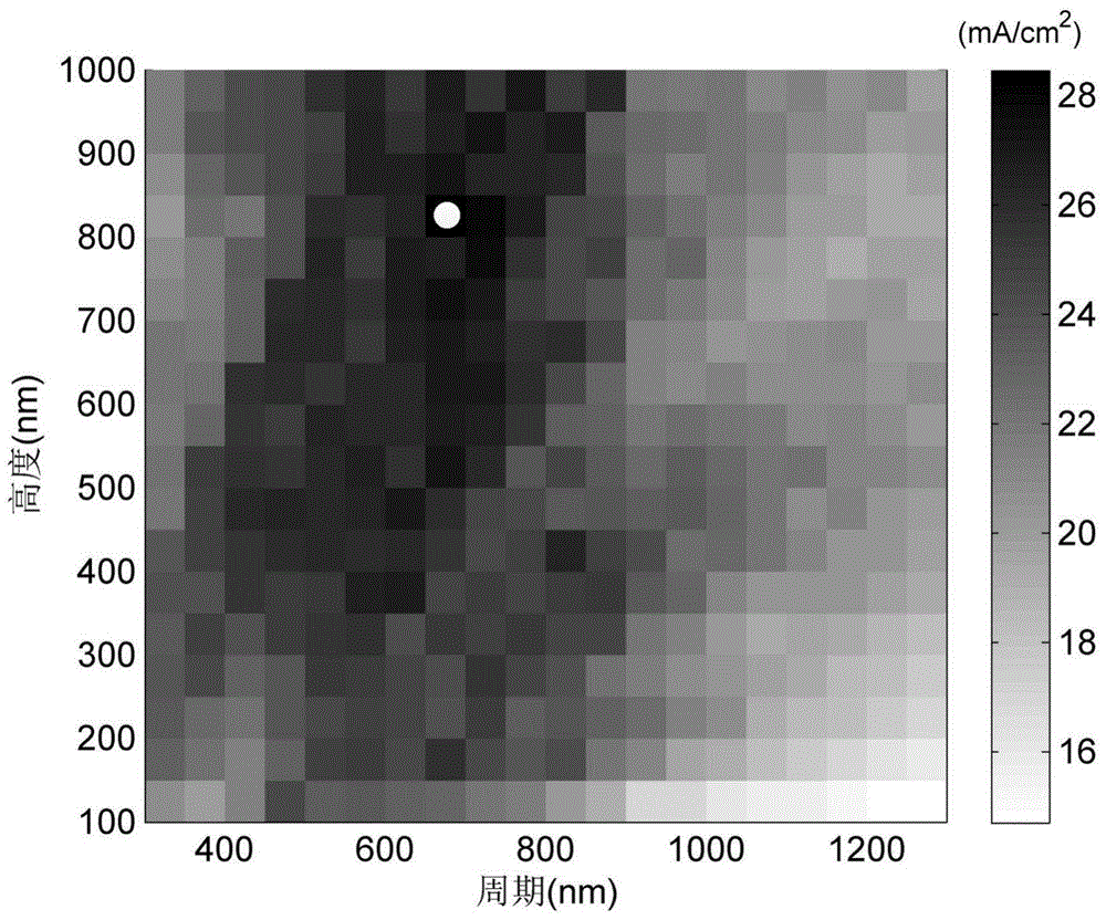
[0027] We give the battery structure (see figure 1 with figure 2 The thickness of the silicon absorption layer of) is 1000nm. Because the two-dimensional light trapping structure of different periods and heights has different effects on the absorption enhancement, the period P varies from 300nm to 1300nm and the height H varies from 100nm at normal incidence. The short-circuit current density corresponding to different light trap structures up to 1000nm J sc (P, H) to optimize the period and height of the periodic two-dimensional light trapping structure.

[0028] Through this optimization method, the two-dimensional cosine waveform surface light trapping structure is optimized, such as image 3 As shown, the period and height of the best two-dimensional cosine wave surface trapping structure are 650nm and 800nm ​​respectively (see image 3 The white point in the middle), the corresponding short-circuit current density is 28.46mA / cm 2 . In the same way, an optimal inverted pyram...


PUM


Abstract

The invention discloses a two-dimension cosine waveform surface light tripping structure and a solar film cell based on the structure. The two-dimension cosine waveform surface light tripping structure comprises a cell absorption layer. The upper and lower surfaces of the cell absorption layer respectively have a cosine waveform light trapping structure. The provided periodic two-dimension cosine waveform surface light tripping structure can be numerically optimized, and is capable of advancing absorption efficiency to a theory limit, thereby improving cell conversion efficiency greatly. Meanwhile, compared with an existing light tripping structure, the periodic two-dimension cosine waveform surface light tripping structure is more practical in production; and the surface type thereof can be prepared through a simple two-beam interference photoetching method, and the formed area is large, and thus the defects of limited area and unordered structure and the like in an existing light tripping structure preparation method can be overcome.

Description

Technical field [0001] The invention relates to the field of new clean energy and micro-nano photonics, in particular to a two-dimensional cosine wave surface light trapping structure and a solar thin film battery based on the structure. Background technique [0002] In today's world, the increasing population and rapid economic development have led to the lack of global conventional energy and serious damage to the ecological environment. Therefore, as a natural, renewable and pollution-free new energy source, solar energy has attracted widespread attention from researchers all over the world. Among them, solar cells that directly convert light energy into clean electrical energy are the most important innovative application. Silicon materials are abundant in nature and have no toxicity to the human body. They are absolutely dominant in solar cell application materials, accounting for more than 98% of the market. Thin-film silicon-based solar cells have become current research...

Claims


Application Information

Patent Timeline
Patent Type & Authority Patents(China)
IPC IPC(8): H01L31/0236
CPCY02E10/50
Inventor 郭小伟刘佳
Owner UNIV OF ELECTRONICS SCI & TECH OF CHINA
Why Eureka
Try Eureka