

Gallium arsenide dual-mode band-pass filter and manufacturing method thereof
A gallium arsenide and filter technology, which is applied in the field of filters, can solve the problems of large radiation loss of filters and unsatisfactory photolithography technology, and achieve the effects of small dielectric loss, miniaturization, and strong coupling characteristics
- Summary
- Abstract
- Description
- Claims
- Application Information
AI Technical Summary
Problems solved by technology
Method used
Image

Examples
Embodiment Construction
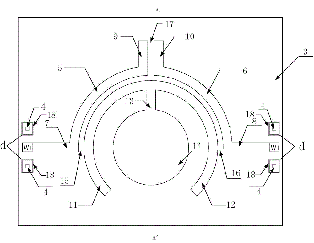
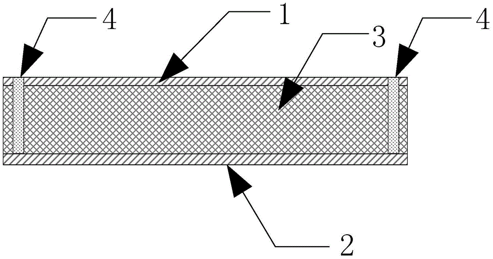
[0021] refer to figure 1 . Embodiments of the dual-mode gallium arsenide filter of the present invention will be described below with reference to the accompanying drawings. In the embodiment described below, the dual-mode gallium arsenide filter mainly includes: a microwave dielectric layer 3, a metal layer 1 formed on the upper surface of the dielectric layer 3, a ground conductor layer 2 formed on the lower surface of the dielectric layer 3, and a ground Hole 4. The metal layer 1 is located on the surface of the dielectric layer 3, and its shape is shown in the figure. The material of the microwave dielectric layer 3 is gallium arsenide, which is located under the metal layer 1 and forms a completely evenly filled rectangular dielectric plate. The microwave dielectric layer 3 is wrapped between the metal layer 1 and the upper and lower surfaces of the ground conductor layer 2 . The ground conductor layer 2 is located on the lower surface of the dielectric layer 3 , has ...
PUM
| Property | Measurement | Unit |
|---|---|---|
| Characteristic impedance | aaaaa | aaaaa |
| Line width | aaaaa | aaaaa |
| Width | aaaaa | aaaaa |
Abstract
Description
Claims
Application Information