Method of restraining notch appearing at bottom of hole during etching process, and hole forming method

A technology for etching holes and gaps, which is used in semiconductor/solid-state device manufacturing, electrical components, circuits, etc., and can solve problems such as deterioration of device performance, damage to shape, and processing process problems.

Active Publication Date: 2016-03-02
ADVANCED MICRO FAB EQUIP INC CHINA
View PDF5 Cites 4 Cited by
  • Summary
  • Abstract
  • Description
  • Claims
  • Application Information

AI Technical Summary

Problems solved by technology

[0003] In some applications, the notch should be avoided as much as possible, because the presence of the notch itself has destroyed the shape of the feature (ie hole

Method used


Image

  • Method of restraining notch appearing at bottom of hole during etching process, and hole forming method
  • Method of restraining notch appearing at bottom of hole during etching process, and hole forming method
  • Method of restraining notch appearing at bottom of hole during etching process, and hole forming method

Examples


Embodiment Construction

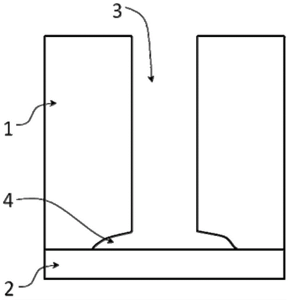
[0024] The current research theory generally believes that in plasma etching, the generation of notching at the bottom of the hole is directly related to the accumulation of charges on silicon (or other materials). Therefore, the idea of ​​suppressing the notch phenomenon is usually to neutralize the accumulated charges on the silicon surface. , or directly reduce the amount of charge that ions transfer to silicon. Specific measures include reducing the frequency of the radio frequency (lower frequency), applying pulsed generators to the radio frequency power supply, and reducing the duty cycle (duty cycle, also known as the duty cycle) and so on.

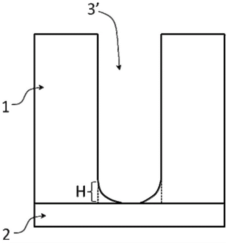
[0025] While studying the subject of notch elimination, the inventors discovered a new factor that can affect the notch: the gas pressure of plasma etching. When other parameters remain unchanged, the lower the working air pressure, the more obvious the improvement of the notch phenomenon.

[0026] In plasma etching, the surface of...


PUM


Abstract

The invention provides a method of restraining a notch appearing at the bottom of a hole during an etching process, and a hole structure forming method. The hole structure forming method mainly comprises the following steps: (1) a substrate is provided, wherein the substrate comprises an to-be-etched material layer and an insulated layer attached to the lower surface of the to-be-etched material layer; (2) the to-be-etched material layer is subjected to anisotropic plasma etching, and a hole is formed initially; and (3) in a relatively-low working air pressure environment, anisotropic plasma etching is continued to deepen the hole. At least when the process of deepening the hole is over, the insulated layer can be exposed through the hole.

Description

technical field [0001] The present invention relates to the field of semiconductor manufacturing, and in particular to a method of using plasma to etch in a material layer to be etched to form a through hole penetrating through the material layer, which is used to suppress the gap at the bottom of the through hole (that is, the intersection between the material layer and the lower insulating layer). interface) there is a phenomenon of notching. Background technique [0002] It is one of the most common processes in semiconductor processing to form via holes in material layers by means of anisotropic plasma etching. Such as figure 1 When etching silicon (or other materials) 1 , due to the electrical isolation of the underlying insulating layer (such as silicon oxide) 2 , a large amount of charges will accumulate on the silicon 1 . Due to the influence of charges, when the etching reaches the interface between the silicon 1 and the insulating layer 2 , notches 4 will be gene...

Claims


Application Information

Patent Timeline
IPC IPC(8): H01L21/768
Inventor 黄秋平王红超严利均刘身健倪图强
Owner ADVANCED MICRO FAB EQUIP INC CHINA
Why Eureka
Try Eureka