Dry etching preparation method of T-shaped hole of integrated circuit

A technology of dry etching and integrated circuits, which is applied in the manufacture of circuits, electrical components, semiconductors/solid-state devices, etc., and can solve problems such as expensive, increased company costs, and inapplicability

Inactive Publication Date: 2016-07-06
YANGZHOU GUOYU ELECTRONICS
View PDF4 Cites 4 Cited by
  • Summary
  • Abstract
  • Description
  • Claims
  • Application Information

AI Technical Summary

Problems solved by technology

For semiconductor manufacturing companies, it is very expensive to purchase equipment or increase the cavity, which increases the cost of the company
This processing method is generally used for 0.6um process platform, and it is not applicable for thinner line width

Method used


Image

  • Dry etching preparation method of T-shaped hole of integrated circuit
  • Dry etching preparation method of T-shaped hole of integrated circuit
  • Dry etching preparation method of T-shaped hole of integrated circuit

Examples


Embodiment Construction

[0019] Aiming at the above-mentioned technical solution, a preferred embodiment is given and described in detail with reference to the drawings.

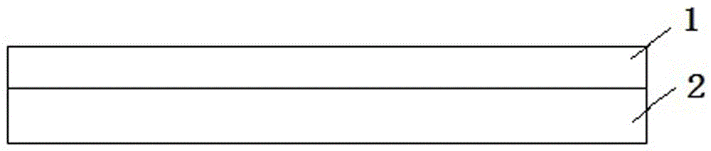
[0020] First, see figure 1 , Deposit isolation dielectric 2 for metal interconnection on doped silicon substrate or isolation dielectric 1 formed by atmospheric pressure CVD deposition, isolation dielectric 2 is deposited by plasma deposition (PECVD), and control isolation dielectric 2 The thickness is 2.3 microns, which is used as a semiconductor substrate for making T-shaped holes.

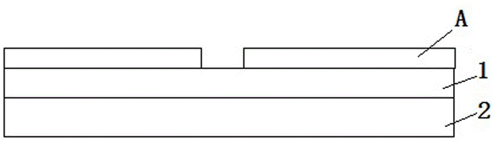
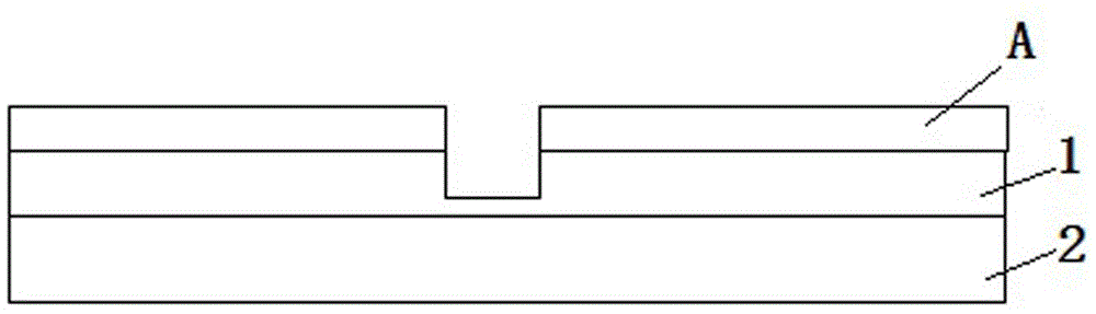
[0021] Step 1), one photolithography, to make fine hole etching window, see figure 2 , a photolithography is performed on the isolation dielectric layer for metal interconnection to make a fine hole etching window. The specific steps are:

[0022] Uniform glue, uniform glue adopts 5370 photoresist provided by Kehua photoresist factory to carry out glue uniformity, and the thickness of photoresist A is controlled at 2.8 microns.

[0023] Exposure,...


PUM

PropertyMeasurementUnit
thicknessaaaaaaaaaa
thicknessaaaaaaaaaa

Abstract

The invention provides a dry etching preparation method of a T-shaped hole of an integrated circuit. The method comprises the following steps: (1) manufacturing of a micropore etching window, carrying out primary photoetching on an isolation medium layer for metal interconnection and manufacturing the micropore etching window; (2) primary etching, carrying out micropore primary etching by an anisotropic plasma dry etching process, wherein the micropore depth after primary etching is smaller than the thickness of the isolation medium layer; and the difference between the thickness of the isolation medium layer and the depth of a micropore after primary etching is equal to the thickness of a macropore of the T-shaped hole; (3) manufacturing of a macropore etching window, carrying out degumming by a plasma dry degumming technology to form a macropore etching window; (4) secondary etching, carrying out secondary etching by the etching technology same as that in the step (2), wherein the secondary etching time is shorter than the primary etching time; and (5) degumming, removing a photoresist by the plasma dry degumming technology. The preparation method is simple; and etching of the T-shaped hole can be finished only by one piece of etching equipment, so that the production cost is reduced.

Description

technical field [0001] The invention relates to the field of semiconductor manufacturing, in particular to an etching preparation process for T-shaped holes in integrated circuit manufacturing. Background technique [0002] In integrated circuit manufacturing, as the size of the device decreases, the size of the lead hole in the back-end process also decreases, but the thickness of the dielectric does not become thinner, forming a lead hole with a high aspect ratio. As a result, the metal is difficult to fill in the lead hole, forming a void. cause device reliability problems. In order to solve this problem, the contact hole of the metal interconnection generally adopts a "T" structure at present. At present, there are two methods for making T-shaped holes. The first one is to use an isotropic etching machine or chamber for wet etching to etch a "bowl"-shaped hole; The etching machine or cavity of the opposite sex is used for etching, and the straight holes are etched. D...

Claims


Application Information

Patent Timeline
Patent Type & Authority Applications(China)
IPC IPC(8): H01L21/311G03F7/36
CPCH01L21/311G03F7/36H01L21/31138H01L21/31144
Inventor 张龙徐海飞王秋建
Owner YANGZHOU GUOYU ELECTRONICS
Why Eureka
Try Eureka