Formation of removable shroud by anisotropic plasma etch

a plasma etch and anisotropic technology, applied in the direction of semiconductor devices, basic electric elements, electrical equipment, etc., can solve the problems of less dense cvd-deposited oxides and comparably poor insulation characteristics

Inactive Publication Date: 2005-12-29
CHANG LIAO HLDG
View PDF3 Cites 5 Cited by
  • Summary
  • Abstract
  • Description
  • Claims
  • Application Information

AI Technical Summary

Benefits of technology

[0013] In accordance with yet another embodiment of the present invention, a method of manufacturing a semiconductor device is disclosed, further comprising: providing an anti-reflective coating (ARC) layer conformally over the dielectric and the silicon oxide layer; and

Problems solved by technology

On the other hand, CVD-deposited oxides tend to be less den

Method used


Image

  • Formation of removable shroud by anisotropic plasma etch
  • Formation of removable shroud by anisotropic plasma etch
  • Formation of removable shroud by anisotropic plasma etch

Examples


Embodiment Construction

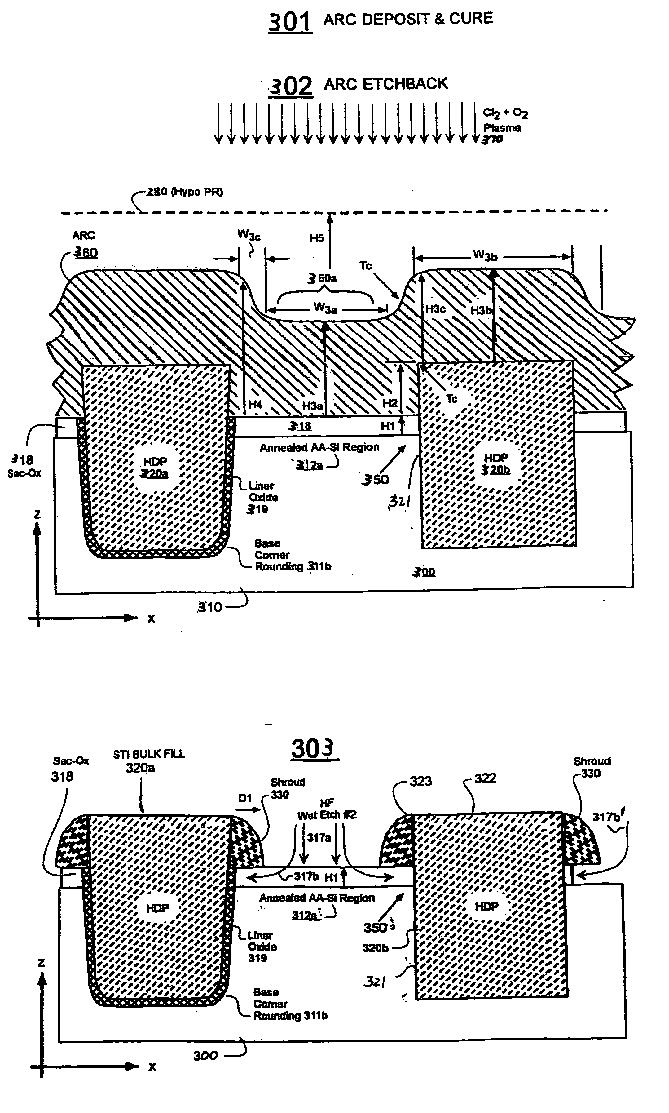
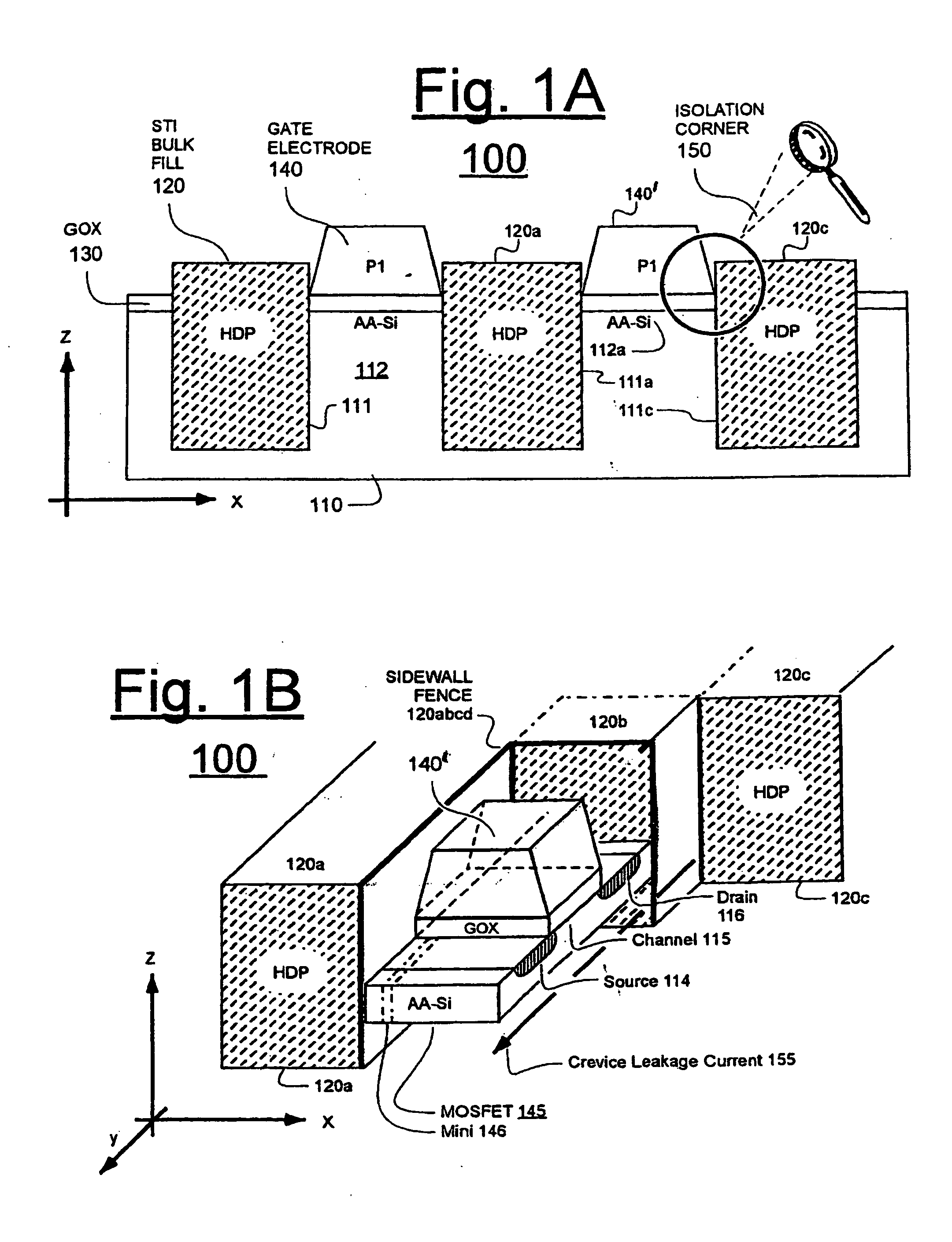
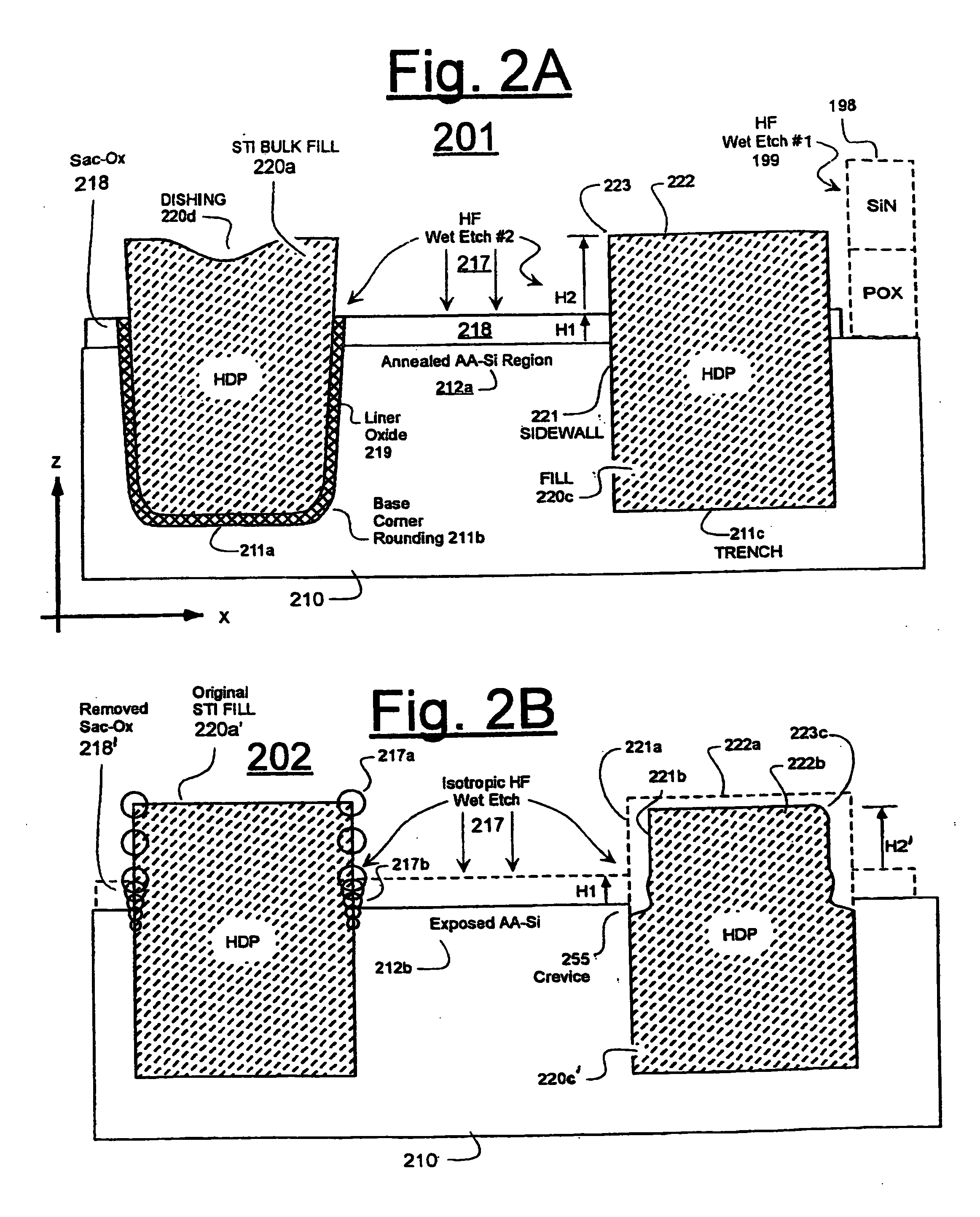
[0028]FIG. 1A is a schematic cross sectional view of a monolithically integrated circuit 100 which relies on STI (where the reliance is at least partial) to provide electrical isolation between active devices. More specifically, a substrate 110 composed of, for example, monocrystalline silicon, has a plurality of spaced-apart isolation trenches 111 formed therein to define gaps between active area mesas 112. So-called active area regions (AA) 112a at the top of the mesas are often used to define critical parts of active devices such as MOSFETs.

[0029] The isolation trenches are typically filled with a bulk insulative material 120 such as HDP-oxide. A gate oxide layer (GOX) 130 is provided on the AA regions 112a so as to abut against the sidewalls of the oxide in the surrounding trenches 111. Gate electrodes such as ones composed of conductive polysilicon (e.g., P1 electrode 140) are provided on the GOX 130. Edges of these gate electrodes 140, 140′ may also abut against the sidewalls...


PUM


Abstract

Isotropic etching of sacrificial oxide that is adjacent to a trench fill step in an STI wafer can lead to undesired etching away of a sidewall of the trench fill material (e.g., HDP oxide). A sidewall protecting method conformably coats the trench fill step and sacrificial oxide with an etch-resistant carbohydrate. In one embodiment, conforming ARC fluid is spun-on and hardened. A selective, dry plasma etches the hardened ARC over the sacrificial oxide while leaving intact part of the ARC that adheres to the trench fill sidewall. The remnant sidewall material defines a protective shroud which delays the subsequent isotropic etchant (e.g., wet HF solution) from immediately reaching the sidewall of the trench fill material. The delay length of the shroud can be controlled by tuning the etchback recipe. In one embodiment, the percent oxygen in an O2 plus Cl2 plasma and/or bias power during the plasma etch is used as a tuning parameter.

Description

BACKGROUND [0001] 1. Field of Disclosure [0002] The present disclosure of invention relates generally to the manufacture of trench-isolated semiconductor devices such as DRAM cells which may be provided in a memory integrated circuit. [0003] The disclosure relates more specifically to certain manufacturing steps by which a juncture between trench isolation and active semiconductor may be prevented from grooving due to an isotropic etch process. [0004] 2. Description of Related Art [0005] So-called shallow trench isolation (STI) has come into common usage for providing electrical isolation between transistors and / or other active devices of a monolithically integrated circuit. STI is particularly useful in situations where low current leakage is important such as in the fabrication of dynamic random access memory (DRAM) devices. [0006] The basic STI process often starts with a monocrystalline semiconductor wafer (e.g., silicon). Pad oxide and silicon nitride layers are usually formed ...

Claims


Application Information

Patent Timeline
IPC IPC(8): H01L21/28H01L21/311H01L21/336H01L21/76H01L21/762H01L21/8234
CPCH01L21/28123H01L21/28238H01L21/823481H01L21/31144H01L21/76224H01L21/31138
Inventor LEE, JOHNHASELDEN, BARBARA A.
Owner CHANG LIAO HLDG
Why Eureka
Try Eureka