Communication device and circuit board module thereof

A technology of circuit board components and communication equipment, which is applied in the direction of electrical components, printed circuits, printed circuits, etc., can solve problems such as complicated wiring, increased circuit board manufacturing costs, and increased circuit board wiring length, so as to reduce costs and reduce Effect of wiring area

Active Publication Date: 2016-03-02
HUIZHOU TCL MOBILE COMM CO LTD
View PDF5 Cites 10 Cited by
  • Summary
  • Abstract
  • Description
  • Claims
  • Application Information

AI Technical Summary

Problems solved by technology

This leads to an increase in the length of the wiring on the circuit board and an increase in the manufacturing cost of the circuit board. A large number of metal traces are printed on the surface of the circuit board and pass through the surrounding area covered by the entire shielding cover, occupying a large amount of space in the inner layer of the PCB. The lines are complicated, the space utilization rate is small, and the aesthetics is also greatly reduced

Method used


Image

  • Communication device and circuit board module thereof

Examples


Embodiment Construction

[0018] In order to make the object, technical solution and advantages of the present invention more clear, the present invention will be further described in detail below in conjunction with the accompanying drawings and embodiments. It should be understood that the specific embodiments described here are only used to explain the present invention, not to limit the present invention.

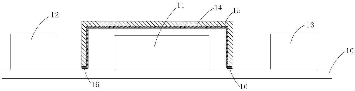
[0019] refer to figure 1 The circuit board assembly of the embodiment of the present invention includes a circuit board 10, a first electronic component 11 disposed on the circuit board 10, a second electronic component 12, a third electronic component 13, and an electromagnetic shield 14, and the electromagnetic shield 14 separates the first An electronic component 11 is housed therein, and the second electronic component 12 and the third electronic component 13 are respectively located on two sides of the first electronic component 11 and are electrically connected by wires 15 . Preferably, t...


PUM


Abstract

The invention discloses a circuit board module. The circuit board module comprises a circuit board, and a first electronic component, a second electronic component and a third electronic component that are arranged on the circuit board, and an electromagnetic shielding cover; the first electronic component is covered by the electromagnetic shielding cover; the second electronic component and the third electronic component are positioned on the two sides of the first electronic component respectively and are electrically connected through wires. The invention also discloses a communication device. According to the circuit board module, the printed circuit wiring on the circuit board is reduced, the wiring area on the circuit board is reduced, the existing wiring space is fully utilized, and the cost of the circuit board is reduced without influencing the PCB appearance and the electromagnetic shielding property of electromagnetic sensitive electronic components.

Description

technical field [0001] The invention relates to the design field of a circuit board and its wiring, in particular to a communication device and a circuit board assembly thereof. Background technique [0002] In order to pursue the compact design of electronic products, in circuit board design, due to the large number of components on the circuit board and the small area of ​​the circuit board, the space for circuit wiring is very small. If there is insufficient space for circuit traces, it needs to be solved by adding layers to the circuit board. This design is not conducive to reducing product cost and manufacturing difficulty. [0003] At present, some electromagnetically sensitive electronic components need to be equipped with shielding shells to prevent electromagnetic interference. In order to reduce the impact on the electronic components as much as possible, other electronic components and circuit wiring must bypass this electronic component, or be distributed separat...

Claims


Application Information

Patent Timeline
IPC IPC(8): H05K1/18H05K9/00
CPCH05K1/181H05K9/0024H05K2201/0707
Inventor 尹协邦
Owner HUIZHOU TCL MOBILE COMM CO LTD
Why Eureka
Try Eureka