Array substrate, preparing method thereof, and display panel
A technology of array substrates and substrate substrates, which is applied in semiconductor/solid-state device manufacturing, instruments, semiconductor devices, etc., and can solve the problems of large opaque area, occupying the area of array substrates, and narrow grid lines.
- Summary
- Abstract
- Description
- Claims
- Application Information
AI Technical Summary
Problems solved by technology
Method used
Image


Examples
preparation example Construction
[0058] On the basis of the above, an embodiment of the present invention also provides a method for preparing the above-mentioned array substrate 01, and the method includes:
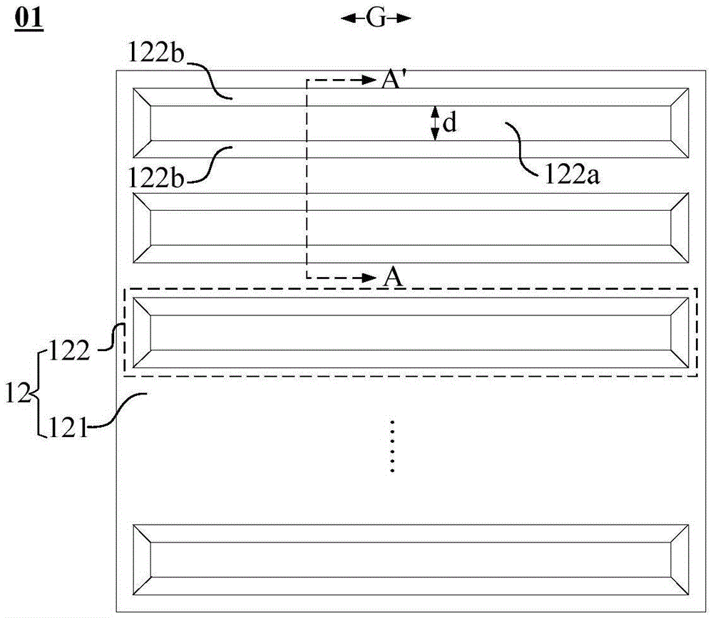
[0059] An isolation layer 12 is formed on the base substrate 11 , and the formed isolation layer 12 includes: a main body layer 121 parallel to the base substrate 11 , and a plurality of protrusions 122 arranged on the main body layer 121 parallel to the gate lines.
[0060] A row of TFTs 13 and a grid line 14 arranged along the grid line direction are formed on at least one side 122b of the two opposite side surfaces 122b of the protruding portion 122 extending along the grid line direction; wherein the TFT 13 and the grid line are formed The side surface 122b of 14 is an inclined surface disposed upward relative to the main body layer 121 .
[0061] Further, the embodiment of the present invention provides two embodiments with different TFT structures, so as to describe the above-mentioned array subst...
Embodiment 1
[0063] refer to image 3 and Figure 4As shown, the protruding portion 122 has a top surface 122a disposed between the two opposite sides and away from the main body layer 121; the array substrate 01 specifically includes: isolating the active layer 132 of the TFT 13 and the gate 131 of the TFT 13 The gate insulating layer 15; the interlayer insulating layer 16 of the source 133, the drain 134 and the gate 131 of the isolation TFT13; wherein, the gate line 14 corresponds to the gate 131 of the active layer 132 is the gate 131 of the TFT13; The pattern 132 is a U-shaped low-temperature polysilicon active layer; the pattern of the active layer 132 spans the main body layer 121, the slope (that is, the side 122b provided with the above-mentioned TFT 13 ) and the top surface 122a; wherein, the U-shaped two sides of the active layer 132 The gate insulating layer 15 covers the active layer 132, and the gate line 14 is located on the area where the gate insulating layer 15 covers th...
Embodiment 2
[0093] like Figure 8 and Figure 9 As shown, the protruding part 122 has a top surface 122a disposed between the two opposite sides and away from the main body layer 121; The gate line 14 connected to the pole 131; the gate insulating layer 15 covering the isolation layer 12; the active layer 132 of amorphous silicon (a-Si) material opposite to the gate 14 on the gate insulating layer 15; and the active layer 132 The source electrode 133 directly in contact with the drain electrode 134 and the data line 23 connected to the source electrode 133 .
[0094] It should be noted that, since at least one side 122b of the two opposite side surfaces 122b extending along the grid line direction of the protruding portion 122 is an upwardly disposed slope relative to the main body layer 121, the protruding portion 122 is far away from the main body layer 121 The top surface 122a should be smaller than the bottom surface near the main body layer 121, that is, the protruding portion 122 ...
PUM
| Property | Measurement | Unit |
|---|---|---|
| Maximum thickness | aaaaa | aaaaa |
| Thickness | aaaaa | aaaaa |
| Thickness | aaaaa | aaaaa |
Abstract
Description
Claims
Application Information
 - R&D
- Intellectual Property
- Life Sciences
- Materials
- Tech Scout
- Unparalleled Data Quality
- Higher Quality Content
- 60% Fewer Hallucinations
Browse by: Latest US Patents, China's latest patents, Technical Efficacy Thesaurus, Application Domain, Technology Topic, Popular Technical Reports.
© 2025 PatSnap. All rights reserved.Legal|Privacy policy|Modern Slavery Act Transparency Statement|Sitemap|About US| Contact US: help@patsnap.com