Silicon chip insertion device

A technology for inserting silicon wafers and silicon wafers, which is applied in the field of auxiliary equipment for preparing solar cells, can solve the problems of discontinuity and low slice efficiency, and achieve the effect of small damage and high insert efficiency

Inactive Publication Date: 2016-03-23
SUZHOU BOYANG ENERGY EQUIP
View PDF4 Cites 4 Cited by
  • Summary
  • Abstract
  • Description
  • Claims
  • Application Information

AI Technical Summary

Problems solved by technology

[0005] The invention patent application with the publication number CN103681968A discloses an automatic wafer inserting machine, which uses a suction cup to grab silicon wafers for splitting and inserting. There is a problem of low fragmentation efficiency

Method used


Image

  • Silicon chip insertion device
  • Silicon chip insertion device
  • Silicon chip insertion device

Examples


Embodiment

[0030] Embodiment: silicon wafer insertion device

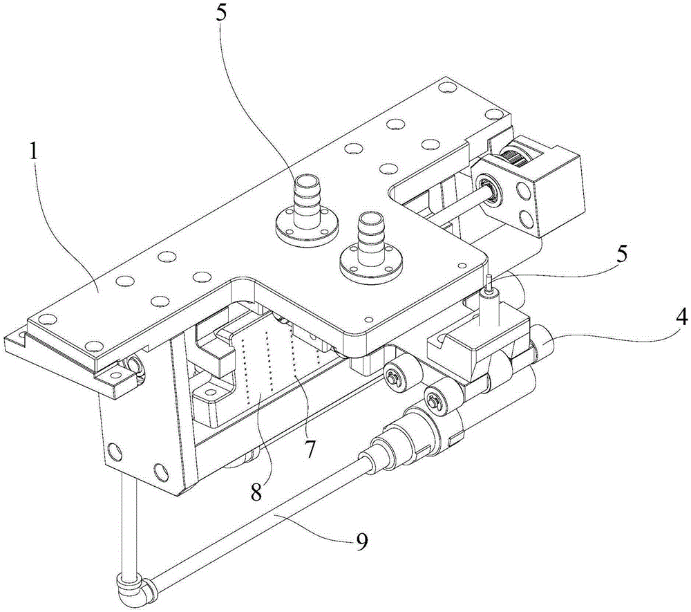
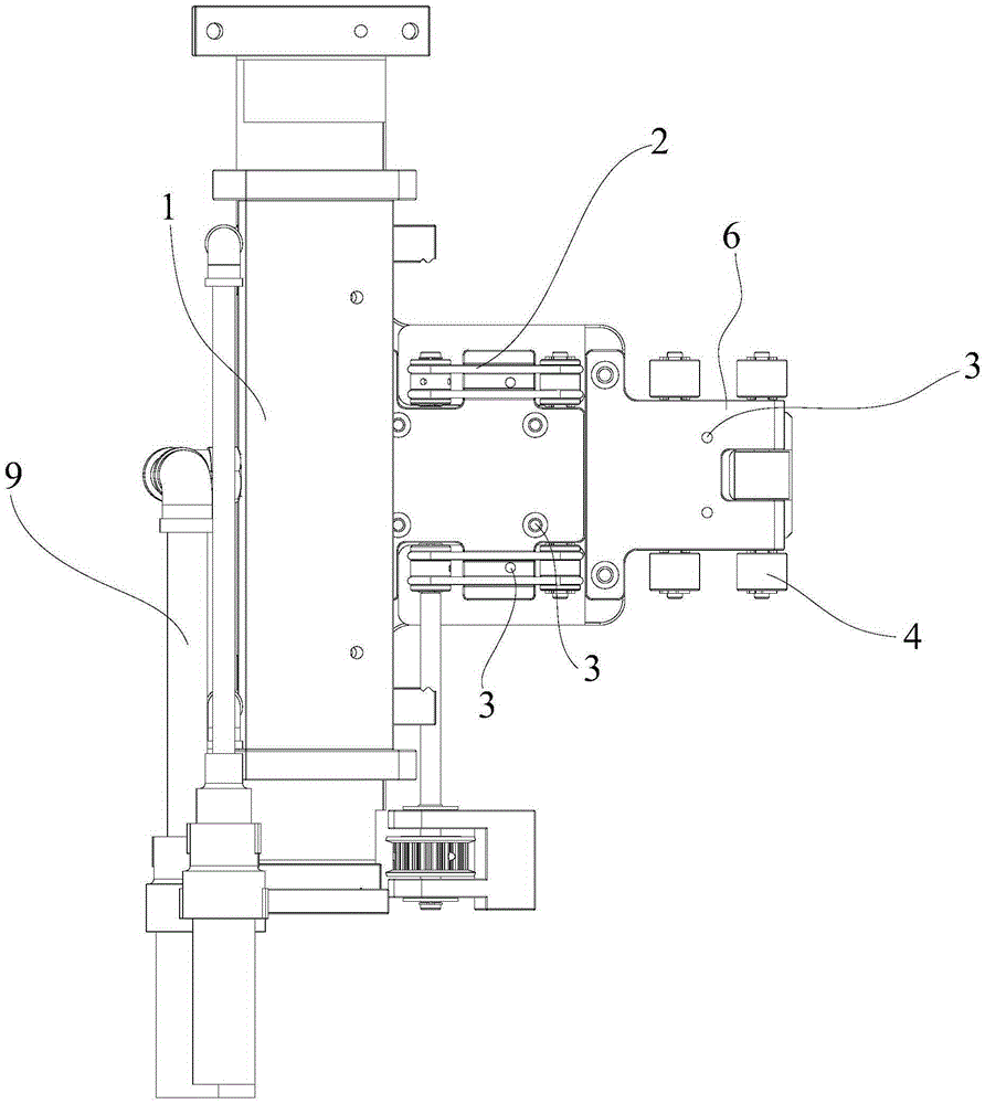
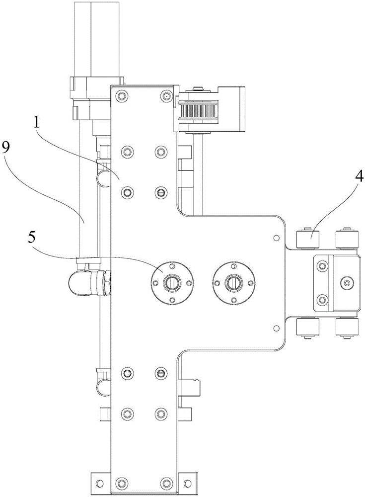
[0031] See attached Figure 1-8 As shown, a silicon wafer inserting device includes a slicer mechanism 10, a feeding chute and a conveyor belt.

[0032] Slicing mechanism 10 comprises silicon chip slicing mechanism body 1, and this silicon chip slicing mechanism body 1 is provided with two parallel and spaced apart slicing conveyor belts 2 downwards, and described silicon chip slicing mechanism body 1 faces the The piece conveyor belt 2 is provided with an air extraction hole 3, which communicates with an air extraction device (not shown in the figure) through a pipeline, and the air extraction device may be a vacuum air extraction device. The front end of the silicon chip slicing mechanism body 1 corresponding to the conveying direction of the slicing conveyor belt 2 is provided with a roller 4; The air hole 7 is communicated with the blowing device (not shown in the figure) through the pipeline 9 . The blowing device can...


PUM


Abstract

A silicon chip insertion device comprises a chip separating mechanism, a feeding trough and conveyor belts. The chip separating mechanism comprises a chip separating mechanism body. Two separated chip conveyor belts which are parallelly and separately arranged are configured below the chip separating mechanism body. The chip separating mechanism body is provided with air exhausting holes in a manner of facing the separated chip conveyor belts. The air exhausting holes are communicated with an air exhausting device through pipeline. The chip separating mechanism body is provided with rollers at positions which correspond with the front end of the conveying direction of the separated chip conveyor belts. The chip separating mechanism body is provided with air blowing holes of which the air blowing direction faces the separated chip conveyor belts. The air blowing holes are communicated with an air blower through pipeline. The feeding trough comprises a feeding trough body and a water pump. The feeding trough body accommodates liquid. The depth of the liquid is always larger than the height of stacked silicon chips. The conveyor belts comprise a first conveyor belt, a second conveyor belt, a third conveyor belt and a fourth conveyor belt. The silicon chip insertion device has advantages of high silicon chip insertion efficiency and small silicon chip damage in silicon chip insertion.

Description

technical field [0001] The invention relates to a silicon wafer inserting device, which belongs to the field of auxiliary equipment for preparing solar cells. Background technique [0002] Since the beginning of the 21st century, global energy consumption has risen sharply, and traditional fossil energy has been increasingly exhausted. Energy issues and environmental issues have gradually become two major issues of global concern. Under the pressure of sustainable development, major countries have listed the solar photovoltaic industry as the focus of the development and utilization of renewable energy. With my country becoming the second largest economy in the world, in October 2013, China's oil imports in October reached 6.3 million barrels per day, surpassing the 6.24 million barrels per day of the United States, replacing the United States as the world's largest net oil importer for the first time. In 2013, China's foreign dependence on oil and natural gas reached 58.1%...

Claims


Application Information

Patent Timeline
IPC IPC(8): H01L31/18H01L21/677
CPCH01L21/677H01L31/18Y02P70/50
Inventor 邱文良
Owner SUZHOU BOYANG ENERGY EQUIP
Why Eureka
Try Eureka