Sample treatment device

A sample processing and sample technology, applied in the field of sample processing devices, can solve the problems of excessive grinding, scrapped samples, difficult grinding, etc., and achieve the effect of easy grinding and not easy to lose

Inactive Publication Date: 2016-03-30
WUHAN XINXIN SEMICON MFG CO LTD
View PDF4 Cites 0 Cited by
  • Summary
  • Abstract
  • Description
  • Claims
  • Application Information

AI Technical Summary

Problems solved by technology

[0005] 2. The ultra-small size sample has been cut from the whole wafer. This situation is difficult to deal with. Because the sample size is too small, subsequent processing is very difficult.
This kind of sample is also difficult to handle, and because the sample size is too small, it is also very difficult to process the sample later
[0007] For the grinding of ultra-small samples in the above 2 and 3 situations, the current processing method can only be controlled by personal experience. However, because the sample size is too small, the processing process is extremely difficult, especially when the target address is in ultra-small samples. Grinding is more difficult at the edge. Despite careful operation, excessive grinding often occurs, resulting in the scrapping of the sample; in addition, the sample size is too small, and the probability of loss during the sample drying and moving process is also higher than that of conventional samples. high

Method used


Image

  • Sample treatment device
  • Sample treatment device
  • Sample treatment device

Examples


Embodiment Construction

[0029] The present invention will be further described below in conjunction with the accompanying drawings and specific embodiments, but not as a limitation of the present invention.

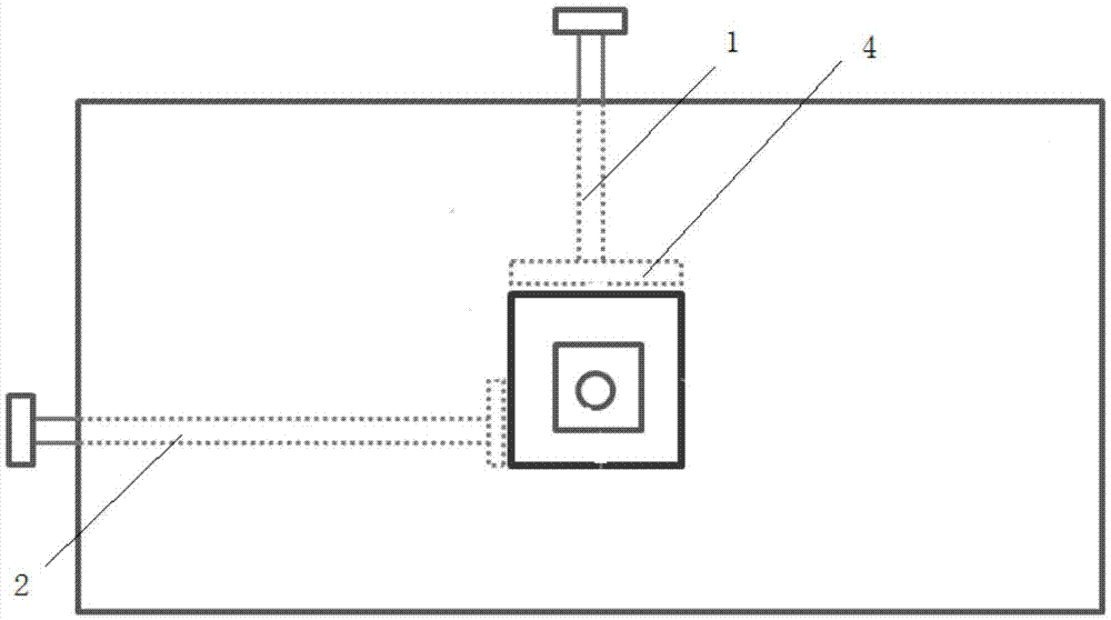
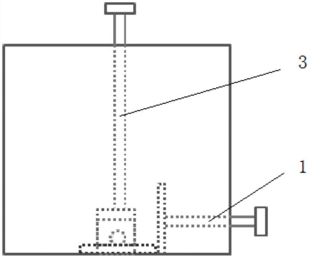
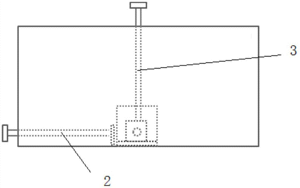
[0030] At present, semiconductor samples need to be processed when doing failure analysis of semiconductor samples, but some semiconductor samples are small in size, or very small, and it is very difficult to grind these small-sized samples, so according to the current operation, rely on Personal experience to control the grinding can easily lead to problems with the uniformity of the grinding cloth. Moreover, if the edge of the sample is ground, it will be more difficult to control, which will easily lead to the scrapping of the sample, making the failure analysis unable to continue.

[0031] After the failure analysis of the sample, it will be dried with a nitrogen gun. The sample size is small, and it is easy to be blown away by the nitrogen gun, and the problem of loss occurs, which eventual...


PUM


Abstract

The invention relates to the field of semiconductor manufacturing, and in particular relates to a sample treatment device. The sample treatment device fixes a sample to be treated in three directions; the part, which is in contact with the sample to be treated, of each fixing device is made from a silicon material, thus fulfilling an aim of fixing the sample to be treated; furthermore, the sample to be treated cannot be damaged by a metal material; meanwhile, one of the three-dimensional fixing devices is a mechanical structure with an adjustable depth, to control the height of the sample, and two fixing devices are used for fixing the position of the sample; a glass plane is used for guaranteeing the coplanar degree of the sample; on such basis, the sample can be fixed, and the coplanar degree of the sample can be guaranteed; therefore, the aim of easiness in grinding is fulfilled, and the sample is difficult to lose.

Description

technical field [0001] The invention relates to the field of semiconductor manufacturing, in particular to a sample processing device. Background technique [0002] When doing failure mode analysis, samples need to be processed, and the processing of ultra-small samples is more difficult than conventional samples, usually less than 4*4mm is considered an ultra-small sample. The most difficult step in the process is sample grinding. The reason for this is that the sample grinding process needs to be ground very precisely to the level that needs to be analyzed. If the target level is not ground, the failure mode cannot be established. Once the grinding is excessive, the It will lead to the disappearance of the target layer, resulting in the rejection of the target sample, both of which will affect the failure of the failure mode analysis. [0003] At present, when doing sample failure analysis, there are several modes for ultra-small sample grinding: [0004] 1. Ultra-small ...

Claims


Application Information

Patent Timeline
Patent Type & Authority Applications(China)
IPC IPC(8): G01N1/28
CPCG01N1/28G01N1/286G01N2001/2866
Inventor 张顺勇汤光敏高慧敏卢勤
Owner WUHAN XINXIN SEMICON MFG CO LTD
Why Eureka
Try Eureka