sram storage unit and storage array

A storage unit and storage node technology, applied in the semiconductor field, achieves the effect of small circuit area, chip saving and production cost reduction

Active Publication Date: 2018-01-26
SPREADTRUM COMM (SHANGHAI) CO LTD
View PDF6 Cites 0 Cited by
  • Summary
  • Abstract
  • Description
  • Claims
  • Application Information

AI Technical Summary

Problems solved by technology

[0021] Similarly, if charged particles bombard the storage node N0, the same consequences will be caused

Method used


Image

  • sram storage unit and storage array
  • sram storage unit and storage array
  • sram storage unit and storage array

Examples


Embodiment Construction

[0055] In order to make the purpose, features and effects of the present invention more obvious and understandable, the specific implementation manners of the present invention will be described in detail below in conjunction with the accompanying drawings.

[0056] Many specific details are set forth in the following description to facilitate a full understanding of the present invention, but the present invention can also be implemented in other ways than described here, so the present invention is not limited by the specific embodiments disclosed below.

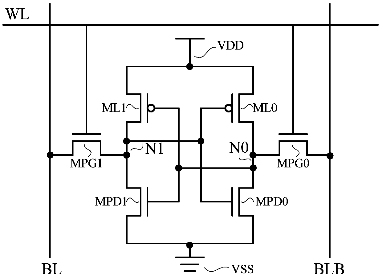
[0057] Such as image 3 The shown SRAM storage unit includes: a first PMOS transistor ML0, a second PMOS transistor ML1, a first dual-gate NMOS transistor MPN0, a second dual-gate NMOS transistor MPN1, a first pass transistor MPG0, a second pass transistor MPG1 and compensation unit. The first pass transistor MPG0 and the second pass transistor MPG1 are PMOS transistors. in:

[0058] The gate of the first PMOS transisto...


PUM


Abstract

The present invention relates to a SRAM (Static random access memory) cell and a memory array. The SRAM memory cell includes a first PMOS (P-channel Metal Oxide Semiconductor) transistor, a second PMOS transistor, a first double-gate NMOS (N-channel metal oxide semiconductor) transistor, a second double-gate NMOS transistor, a first transmission transistor, a second transmission transistor and a compensation unit. The single event upset effect of the SRAM memory cell can be overcome.

Description

technical field [0001] The invention relates to the technical field of semiconductors, in particular to an SRAM storage unit and a storage array. Background technique [0002] SRAM (Static Random Access Memory, hereinafter referred to as SRAM) has the advantages of high speed, low power consumption and compatibility with standard processes. It is widely used in PCs, personal communications, consumer electronics (smart cards, digital cameras, multimedia players) and other fields. [0003] The most common SRAM storage unit is 6T unit, such as figure 1 As shown, the SRAM storage unit includes: a first PMOS transistor ML0, a second PMOS transistor ML1, a first NMOS transistor MPD0, a second NMOS transistor MPD1, a third NMOS transistor MPG0 and a fourth NMOS transistor MPG1. [0004] The first PMOS transistor ML0 , the second PMOS transistor ML1 , the first NMOS transistor MPD0 and the second NMOS transistor MPD1 form a bistable circuit, and the bistable circuit forms a latch ...

Claims


Application Information

Patent Timeline
Patent Type & Authority Patents(China)
IPC IPC(8): G11C11/413
Inventor 王林
Owner SPREADTRUM COMM (SHANGHAI) CO LTD
Why Eureka
Try Eureka