Radiation-proof packaging material for chip and radiation-proof packaging process

A packaging material and packaging process technology, applied in the direction of electrical components, electrical solid devices, circuits, etc., can solve the problems of inability to improve the anti-radiation performance of device plastics, unfavorable integration and portability of aerospace, and difficulty in forming strong connections, etc., to achieve Improve the radiation resistance performance, improve the absorption of radiation energy, and the effect of low cost

Pending Publication Date: 2021-12-17
重庆平创半导体研究院有限责任公司
View PDF1 Cites 0 Cited by
  • Summary
  • Abstract
  • Description
  • Claims
  • Application Information

AI Technical Summary

Problems solved by technology

[0003] The anti-radiation technical solutions in the prior art include coating method, element doping method and shell wrapping method. The coating method needs to generate an anti-radiation layer on the surface of the object. A patent document with the authorized announcement number CN111118455B proposes a By inserting a layer of metal chromium between zirconia and silicon steel, the connection performance between the zirconia layer and silicon steel is improved on the basis of improving the radiation resistance, but the plastic package device is mainly composed of two parts: the bottom copper substrate and the back plastic. The current coating process is mostly metal oxides such as zirconia. It is not easy to form a strong connection between the metal oxide and the plastic of the plastic packaged device, and it cannot improve the radiation resistance of the plastic part of the device.
The element doping method is mostly doping rare earth elements and inorganic non-metallic materials, which have the problems of high price and relatively poor performance.
The final shell wrapping method needs to add an additional layer of structure on the outer layer of the device. In the field of low-energy radiation, although the shell wrapping greatly improves the radiation resistance of the device, it increases the weight and volume, which is not conducive to the lightness of aerospace integration. requirements

Method used


Image

  • Radiation-proof packaging material for chip and radiation-proof packaging process

Examples


Embodiment 1

[0032] A chip anti-irradiation packaging material, weighing 2g of plastic packaging compound and wide bandgap semiconductor particles, doping wide bandgap semiconductor particles in the plastic packaging compound, the plastic packaging material is epoxy molding compound, and the wide bandgap semiconductor particles are silicon carbide wide For the bandgap semiconductor particles, the weight ratio of the silicon carbide wide bandgap semiconductor particles is 20%, that is, the weight of the silicon carbide wide bandgap semiconductor particles is 0.4g, and the particle size of the silicon carbide wide bandgap semiconductor particles is 10nm.

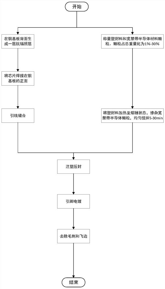
[0033] A chip radiation-resistant packaging process, comprising:

[0034] S1: grow a radiation-resistant layer on the back of the copper substrate, solder the chip on the front of the copper substrate, and bond the chip and the pins of the copper substrate at the same time; wherein, the material of the radiation-resistant layer is zirconia,...

Embodiment 2

[0039] A chip anti-irradiation packaging material, weighing 2g of plastic packaging compound and wide bandgap semiconductor particles, doping wide bandgap semiconductor particles in the plastic packaging compound, the plastic packaging material is epoxy molding compound, and the wide bandgap semiconductor particles are silicon carbide wide For the bandgap semiconductor particles, the silicon carbide wide bandgap semiconductor particles account for 10% by weight, and the particle size of the wide bandgap semiconductor particles is 200nm.

[0040] A chip radiation-resistant packaging process, comprising:

[0041]S1: grow a radiation-resistant layer on the back of the copper substrate, solder the chip on the front of the copper substrate, and bond the chip and the pins of the copper substrate at the same time; wherein, the material of the radiation-resistant layer is zirconia, and the thickness of the radiation-resistant layer is 100um, the area of ​​the anti-radiation layer is t...

Embodiment 3

[0046] A chip anti-irradiation packaging material, weighing 2g of plastic packaging compound and wide bandgap semiconductor particles, doping wide bandgap semiconductor particles in the plastic packaging compound, the plastic packaging material is epoxy molding compound, and the wide bandgap semiconductor particles are silicon carbide wide For the bandgap semiconductor particles, the silicon carbide wide bandgap semiconductor particles account for 35% by weight, and the particle size of the wide bandgap semiconductor is 5um.

[0047] A chip radiation-resistant packaging process, comprising:

[0048] S1: grow a radiation-resistant layer on the back of the copper substrate, solder the chip on the front of the copper substrate, and bond the chip and the pins of the copper substrate at the same time; wherein, the material of the radiation-resistant layer is zirconia, and the thickness of the radiation-resistant layer is 1mm, the area of ​​the anti-radiation layer is the area of ​​...


PUM

PropertyMeasurementUnit
particle diameteraaaaaaaaaa

Abstract

The invention belongs to the technical field of materials for the material nuclear industry, and particularly relates to a chip anti-radiation packaging material and an anti-radiation packaging process. The chip anti-radiation packaging material is formed by doping wide bandgap semiconductor particles in a plastic packaging material, and the weight ratio of the wide bandgap semiconductor particles is 10-75%. The chip anti-radiation packaging process comprises the following steps: firstly, growing an anti-radiation layer on the back surface of a copper substrate, welding a chip on the front surface of the copper substrate, and bonding the chip with a pin of the copper substrate; then weighing a plastic packaging material and the doped particles, putting the plastic packaging material and the doped particles into a mold with a preset stirring temperature, and uniformly stirring, so as to obtain a plastic packaging material composite material after the stirring time is ended; and finally, carrying out injection molding and press sealing on the uniformly stirred plastic packaging composite material, and carrying out pin electroplating and burr and flash removal on the plastic packaged chip. The radiation-proof performance of the whole chip and the reliability in the space environment are improved, and meanwhile, the radiation-proof capability of the back of a chip device is improved.

Description

technical field [0001] The invention belongs to the technical field of materials used in the nuclear industry, and in particular relates to a chip radiation-resistant packaging material and a radiation-resistant packaging process. Background technique [0002] With the progress of the times, our country has made great progress in the field of aviation. From manned spacecraft to Mars exploration, from Tiangong-2 to Beidou global coverage, more and more power devices have been brought to work in space. However, compared with the general working environment, the reliability of power devices in space is very important. Among them, the packaging technology of power devices has greatly improved the reliability of power devices. There are various packaging forms of power devices, among which plastic packaging It has considerable advantages in terms of cost, size, weight, etc., and as the reliability of plastic packaging has been greatly improved in recent years, plastic packaging d...

Claims


Application Information

Patent Timeline
Patent Type & Authority Applications(China)
IPC IPC(8): H01L23/552H01L23/29H01L23/373H01L21/56
CPCH01L23/552H01L23/298H01L23/293H01L23/3738H01L21/56
Inventor 钱靖陈显平罗厚彩
Owner 重庆平创半导体研究院有限责任公司
Why Eureka
Try Eureka