Non-punch-through deep trench IGBT with field stop structure and manufacturing method thereof

A non-punch-through, manufacturing method technology, used in semiconductor/solid-state device manufacturing, electrical components, circuits, etc., can solve the problems of not using high-voltage technology, poor high-voltage withstand performance, and high-frequency application limitations, and achieve easy implementation. , The effect of high short-circuit tolerance and small area

Inactive Publication Date: 2010-09-08
TIANJIN HUANXIN TECH DEV
View PDF7 Cites 25 Cited by
  • Summary
  • Abstract
  • Description
  • Claims
  • Application Information

AI Technical Summary

Problems solved by technology

However, there are still many deficiencies in the IGBT under this patented structure: first, the IGBT under this structure is a punch-through IGBT, and there is a long time delay when the device is turned off, which is limited in high-freque

Method used


Image

  • Non-punch-through deep trench IGBT with field stop structure and manufacturing method thereof
  • Non-punch-through deep trench IGBT with field stop structure and manufacturing method thereof
  • Non-punch-through deep trench IGBT with field stop structure and manufacturing method thereof

Examples


Embodiment Construction

[0029] The present invention will be further described below in conjunction with accompanying drawing and embodiment:

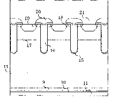
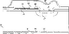
[0030] refer to Figure 1 ~ Figure 3 , a non-punch-through deep trench IGBT with a field stop structure, comprising an NMOS field effect transistor and a PNP bipolar transistor driven by the NMOS field effect transistor; or including a PMOS field effect transistor and a PMOS field effect transistor driven by the PMOS field effect transistor An NPN bipolar transistor driven by a tube, an NMOS field effect transistor or a PMOS field effect transistor includes an emitter electrode, a gate electrode and a silicon substrate body region, and a PNP bipolar transistor or an NPN transistor includes an emitter electrode, a silicon substrate body region and a collector electrode , which is characterized in that: on one side of the silicon substrate body region 12 (close to the gate electrode 3 and the emitter electrode 4), a cell region 1 with a high withstand voltage d...


PUM


Abstract

The invention discloses a non-punch-through deep trench IGBT with a field stop structure and a manufacturing method thereof. The IGBT is equivalent to one NMOS field-effect tube driving one PNP bipolar transistor or one PMOS field-effect tube driving one NPN bipolar transistor. The NMOS tube or the PMOS tube in the invention realizes a vertical gate and a vertical trench through a deep trench technology and a high voltage-resistant trench gate technology is adopted; the NMOS tube or the PMOS tube and the PNP tube or the NPN tube are directly manufactured on a polished wafer to form a non-punch-through IGBT structure; and a field stop layer with the same doping type as a base region and with doping concentration higher than the base region is formed in the base region of the PNP tube or the NPN tube at a position close to a collector region through ion implantation or diffusion. The invention has the advantages that the cost of the manufacturing method is low and the implementation is easy; and the area of the manufactured IGBT is small, the switching loss is small, the short-circuit tolerance is high, the anti-electromagnetic interference capacity and the radiation resistance are enhanced and the like. Thereby, the demand of the market on the high quality of IGBT products is satisfied.

Description

technical field [0001] The invention relates to an IGBT (insulated gate bipolar transistor) structure and a manufacturing method thereof in the field of power devices, in particular to a non-penetrating deep trench IGBT with a field stop structure and a manufacturing method thereof. Background technique [0002] IGBT, or Insulated Gate Bipolar Transistor, is a composite device of MOSFET (Field Effect Transistor) and bipolar transistor. IGBT is mainly used in industrial control, consumer electronics, computer, network communication, automotive electronics and other fields. With the technological development and market demand increase in my country's UHV DC transmission, high-voltage frequency conversion, AC drive locomotives / EMUs, urban rail transit and other fields, the in-depth implementation of new energy, energy conservation and emission reduction national policies, and the arrival of the era of low-carbon economy, frequency conversion New applications such as solar power...

Claims


Application Information

Patent Timeline
IPC IPC(8): H01L29/739H01L29/06H01L29/10H01L29/423H01L21/331
Inventor 饶祖刚丛培金沈浩平冯春阳陆界江赵雁
Owner TIANJIN HUANXIN TECH DEV
Why Eureka
Try Eureka