

Wafer processing method
A processing method and wafer technology, applied in the direction of electrical components, semiconductor/solid-state device manufacturing, circuits, etc., can solve the problems of semiconductor device failure, affecting the performance and reliability of semiconductor devices, semiconductor device structure pollution, etc., to achieve adhesion Enhanced, easy-peel removal
- Summary
- Abstract
- Description
- Claims
- Application Information
AI Technical Summary
Problems solved by technology
Method used
Image

Examples
Embodiment Construction
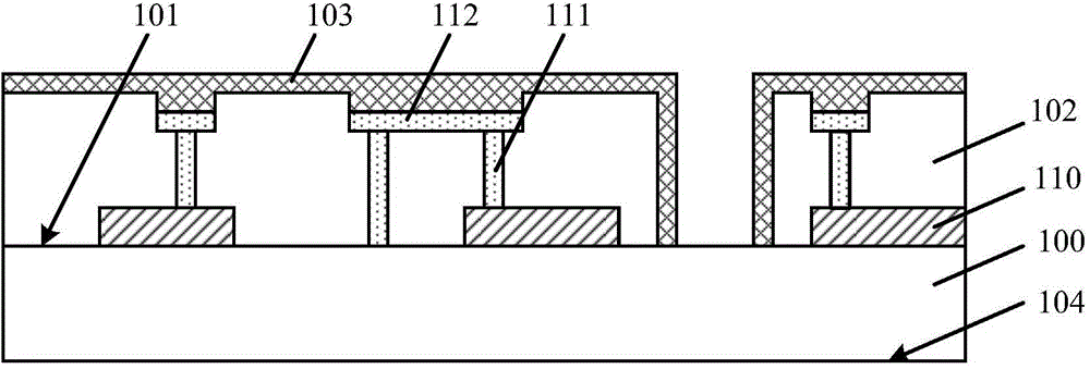
[0031] As mentioned in the background technology, after the protective film is removed by the film removal process, a large amount of attachments will remain on the surface of the semiconductor device structure, which will pollute the semiconductor device structure, affect the performance and reliability of the formed semiconductor device, and even Cause the formed semiconductor device to fail.
[0032] For details, please refer to figure 1 , figure 1 It is a schematic cross-sectional structure diagram of forming a protective film on the surface of a semiconductor device structure located on one side of the wafer according to an embodiment of the present invention, including: a substrate 100; a device structure 110 located on the first surface 101 of the substrate 100; located on the surface of the device structure 110 and The conductive plug 111 on the surface of the substrate 100, the conductive plug 111 is electrically connected to the device structure 110 and the substrat...
PUM
 Abstract
Description
Claims
Application Information