Method for electrochemical polishing of metal interconnection wafer structure

A technology for polishing metal and electrochemistry, applied in the field of electrochemical polishing, can solve the problems of inability to be directly equivalent, the calculation method is not rigorous enough, and the polishing yield is low, and the effect of improving the yield is achieved.

Active Publication Date: 2016-03-30
ACM RES SHANGHAI
View PDF5 Cites 8 Cited by
  • Summary
  • Abstract
  • Description
  • Claims
  • Application Information

AI Technical Summary

Problems solved by technology

This will lead to a consequence: the measured polishing rate RR is different from the polishing rate RR when the wafer product is actually polished, and cannot be directly equated
[0007] Under the co...

Method used


Image

  • Method for electrochemical polishing of metal interconnection wafer structure
  • Method for electrochemical polishing of metal interconnection wafer structure
  • Method for electrochemical polishing of metal interconnection wafer structure

Examples


Embodiment approach

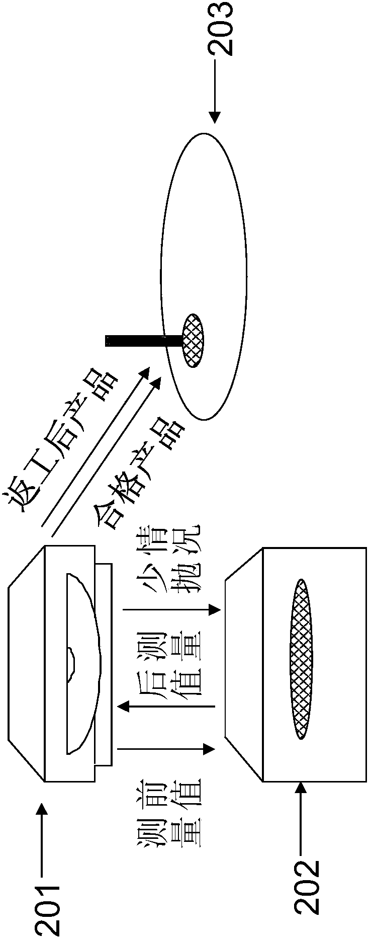
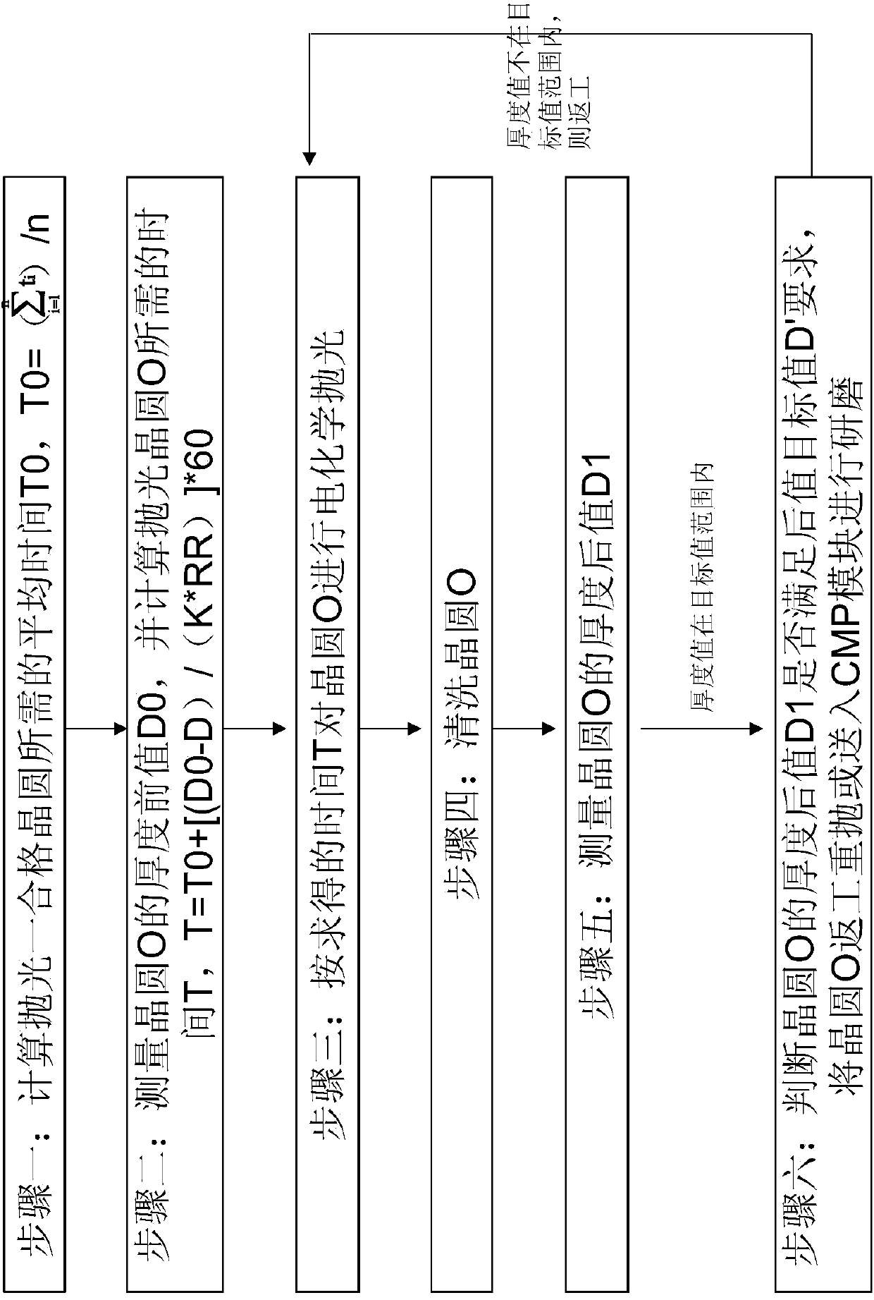
[0052] Step 1: Calculate the average time T0 required for polishing a qualified wafer according to the polishing results of the first N batches, where N=20, T 0 = ( Σ i = 1 n t i ) / n ;

[0053] Step 2: Measure the thickness of wafer O before D0, compare it with the target value D of the previous value, and calculate the required polishing wafer O according to the formula T=T0+[(D0-D) / (K*RR)]*60 time T;

[0054] Step 3: Perform electrochemical polishing on the wafer O according to the obtained time T;

[0055] Step 4: cleaning wafer O;

[0056] Step 5: Measure the thickness D1 of the wafer O;

[0057] Step 6: Determine whether the post-thickness value D1 of the wafer O satisfies the requirement of the post-value target ...


PUM


Abstract

The present invention provides a method for electrochemical polishing of a metal interconnection wafer structure. The method provided by the invention comprises: the step 1, performing electrochemical polishing of one part of wafers in a wafer production, and obtaining an average time T0 being required to polish a qualified wafer; the step 2, measuring the thickness front value D0 of any one wafer O in the wafer production, and comparing the thickness front value D0 with a front value target value D; the step 3, performing electrochemical polishing of the wafer O; the step 4, cleaning the wafer O; the step 5, measuring the thickness back value D1 of the wafer O; the step 6, determining whether the thickness back value D1 of the wafer O meets the requirement of a back value target value D' or not, and reworking the wafer O or putting into a CMP module. The time T (which is required for polishing the wafer O)=T0+[(D0-D)/(K*RR)]*60, wherein RR is polishing rate and K is a constant coefficient; the RR slows down with increasing the batch number of polishing wafers, and the K is determined by the feature of the wafer production. The method for electrochemical polishing of a metal interconnection wafer structure is easy to implement and obvious in effect, and is able to greatly improve the yield rate of high polishing wafer productions.

Description

technical field [0001] The invention relates to the field of electrochemical polishing, more specifically, to a method for electrochemically polishing wafers, and in particular to a process control algorithm for stress-free electrochemically polishing metal interconnected wafer structures. Background technique [0002] In the integrated circuit polishing process, there are many technical means that can be used, which are well known to those skilled in the art and generally include: CMP (Chemical Mechanical Polishing) process or electrochemical polishing process. Among them, there is a unique SFP (stress-free electrochemical polishing) process, which is very suitable for polishing the metal film layer because it hardly generates mechanical force on the wafer surface to damage the wafer during the polishing process. Therefore, it is applied to the polishing of wafer products after electroplating by some manufacturers pursuing high quality, especially for wafer products contain...

Claims


Application Information

Patent Timeline
IPC IPC(8): H01L21/768
Inventor 杨贵璞王坚王晖
Owner ACM RES SHANGHAI
Why Eureka
Try Eureka