Alignment mark for contact hole alignment and forming method thereof

An alignment mark and contact hole technology, applied in electrical components, electrical solid devices, circuits, etc., can solve the problems of decreased alignment quality, difficult to meet requirements, small thickness, etc., to improve alignment quality and increase effective thickness. Effect

Active Publication Date: 2016-03-30
SEMICON MFG INT (SHANGHAI) CORP
View PDF4 Cites 0 Cited by
  • Summary
  • Abstract
  • Description
  • Claims
  • Application Information

AI Technical Summary

Problems solved by technology

Since the thickness of the alignment mark 103 for contact hole alignment is relatively small (usually at left and right), it is often difficult to meet the requirements for alignment of contact holes, resulting in a decline in alignment quality

Method used


Image

  • Alignment mark for contact hole alignment and forming method thereof
  • Alignment mark for contact hole alignment and forming method thereof
  • Alignment mark for contact hole alignment and forming method thereof

Examples


Embodiment 1

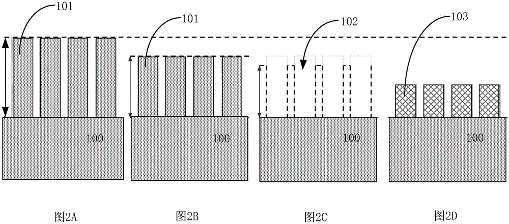
[0040] An embodiment of the present invention provides a method for forming an alignment mark (mark) for contact hole (CT) alignment, and the method includes the following steps:

[0041] Provide semiconductor substrates;

[0042] forming shallow trench isolation on both sides of the region of the semiconductor substrate where an alignment mark for contact hole alignment is to be formed;

[0043] An alignment mark is formed on a region of the semiconductor substrate where an alignment mark for contact hole alignment is to be formed, wherein the alignment mark has the same material as the semiconductor substrate.

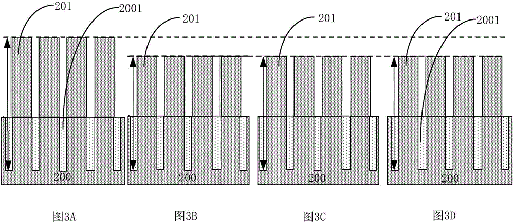
[0044] in, image 3 A specific example of a method for forming an alignment mark for contact hole alignment according to an embodiment of the present invention is shown. Such as image 3 As shown, this specific example includes the following steps:

[0045] Step A1: Provide a semiconductor substrate 200, and form shallow trench isolation (STI) 2001 on both sides of...

Embodiment 2

[0067] An embodiment of the present invention provides an alignment mark for contact hole alignment, which is manufactured by the method described in the first embodiment above.

[0068] Such as Figure 5 As shown, the alignment mark 201 used for contact hole alignment in the embodiment of the present invention is formed on the semiconductor substrate 200, wherein the alignment mark 201 has the same material as the semiconductor substrate 200, and the inside of the semiconductor substrate 200 Shallow trench isolations 2001 located on both sides of the alignment mark 201 are formed.

[0069] Exemplarily, the material of the alignment mark 201 may be polysilicon or other suitable materials. The semiconductor substrate 200 may be a silicon substrate or other suitable substrates. The material of the shallow trench isolation (STI) 2001 can be silicon oxide or other suitable materials.

[0070] Wherein, the alignment mark 201 can be formed in the same process as the dummy gate of...


PUM


Abstract

The invention provides an alignment mark for contact hole alignment and a forming method thereof, and relates to the technical field of semiconductors. The forming method of the alignment mark for contact hole alignment comprises a step of forming shallow trench isolations on the two sides of an area, in which an alignment mark for contact hole alignment is to be formed, on a semiconductor substrate, and a step of forming an alignment mark of the same material as the semiconductor substrate in the area, in which an alignment mark for contact hole alignment is to be formed, on the semiconductor substrate. Therefore, the effective thickness of the alignment mark can be improved, and the quality of alignment can be improved. The alignment mark for contact hole alignment is made of the same material as the semiconductor substrate, and the shallow trench isolations are formed in the areas on the two sides of the alignment mark in the semiconductor substrate, so that the effective thickness of the alignment mark is improved, and the quality of alignment is improved.

Description

technical field [0001] The invention relates to the technical field of semiconductors, in particular to an alignment mark for contact hole (CT) alignment and a forming method thereof. Background technique [0002] In the field of semiconductor technology, in the manufacturing process of semiconductor devices, alignment is one of the most crucial processes among many processes. Among them, the so-called alignment or alignment process refers to recognizing the alignment mark on the surface of the semiconductor substrate through the machine recognition on the lithography equipment or human eyes, so that the back-end process and the front-end process have positional overlap. [0003] As the process nodes of semiconductor technology continue to decrease, the alignment of contact holes (CT) becomes less and less easy to control. When semiconductor technology develops to 28nm and below process nodes, in the manufacturing process of semiconductor devices using high-k metal gate tec...

Claims


Application Information

Patent Timeline
Patent Type & Authority Applications(China)
IPC IPC(8): H01L23/544
Inventor 赵简
Owner SEMICON MFG INT (SHANGHAI) CORP
Why Eureka
Try Eureka