Igfet with silicide contact on ultra-thin gate

a technology of igfet and contact, which is applied in the direction of semiconductor devices, electrical equipment, transistors, etc., can solve the problems of difficult to obtain consistent threshold voltages, poor quality of refractory metal oxides, and inability to provide suitable replacements for polysilicon, etc., to achieve a well-controlled doping profile and high-miniaturized igfet

Inactive Publication Date: 2002-01-10
DAWSON ROBERT +6
View PDF0 Cites 6 Cited by
  • Summary
  • Abstract
  • Description
  • Claims
  • Application Information

AI Technical Summary

Benefits of technology

0018] A key advantage of the invention is that a highly miniaturized IGFET can be provided with an ultra-thin polysilicon gate having

Problems solved by technology

Although refractory metals and their silicides have adequately high melting points, they usually do not provide suitable replacements for polysilicon as the gate.
For instance, the oxides of refractory metals are typically of poor quality, and in some cases volatile (Mo and W oxides).
In addition, it may be difficult to obtain consistent threshold voltages due to impurities in the sources

Method used


Image

  • Igfet with silicide contact on ultra-thin gate
  • Igfet with silicide contact on ultra-thin gate
  • Igfet with silicide contact on ultra-thin gate

Examples


Embodiment Construction

[0022] In the drawings, depicted elements are not necessarily drawn to scale and like or similar elements may be designated by the same reference numeral throughout the several views.

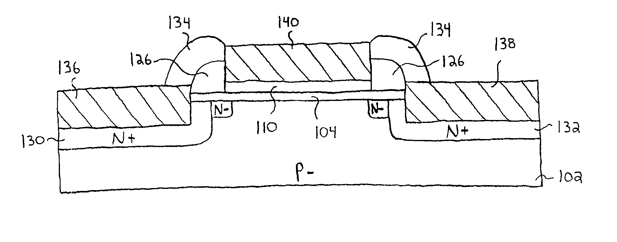
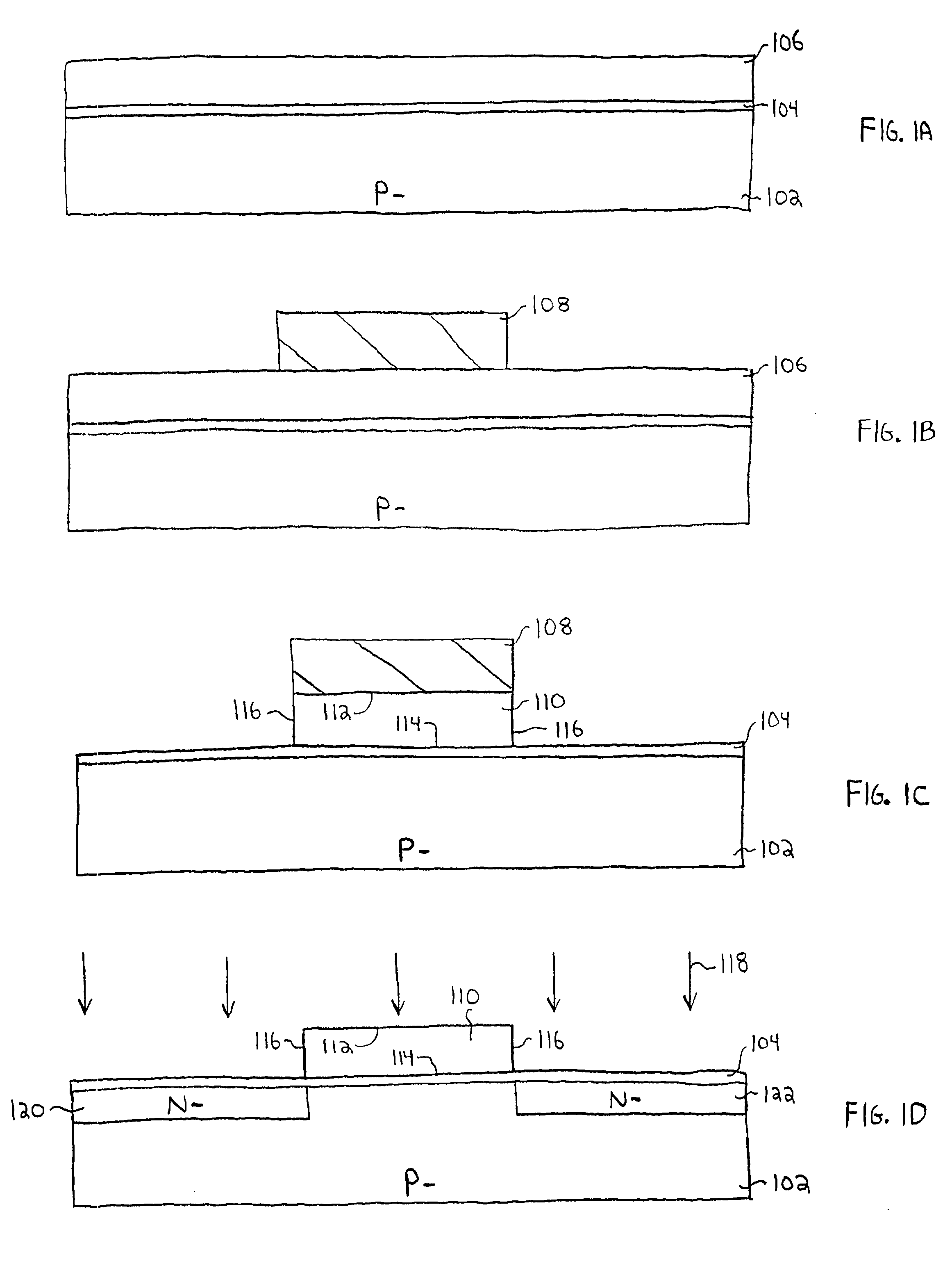
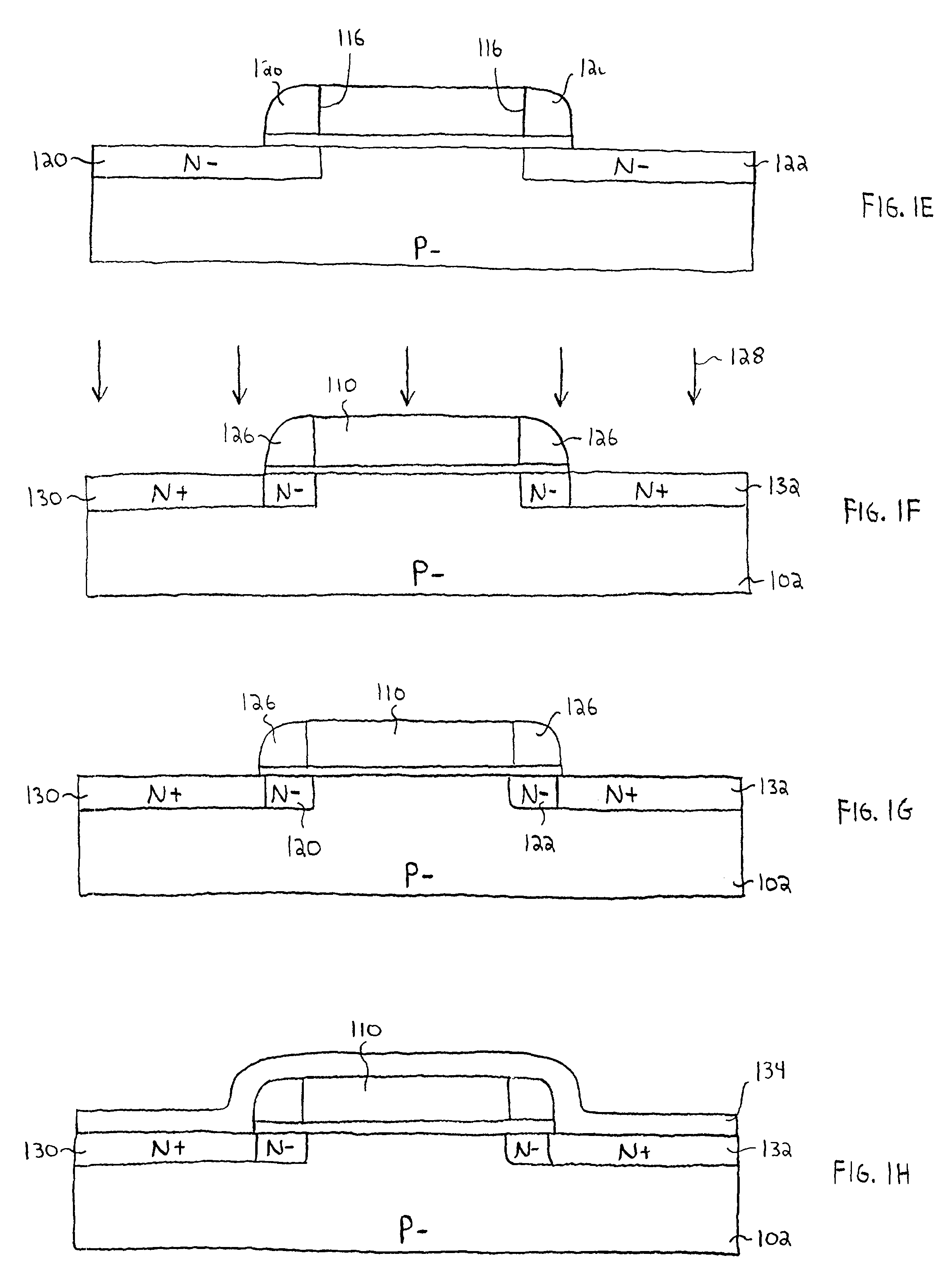
[0023] In FIG. 1A, silicon substrate 102 suitable for integrated circuit manufacture includes a P-type epitaxial surface layer disposed on a P+ base layer (not shown). The epitaxial surface layer provides an active region with a boron background concentration on the order of 1.times.10.sup.16atoms / cm.sup.3, a orientation and a resistivity of 12 ohm-cm. Substrate 102 can be subjected to a threshold voltage implant, a punch-through implant, and a well implant as is conventional. For convenience of illustration, dielectric isolation such as field oxides between adjacent active regions is not shown. A blanket layer of gate oxide 104, composed of silicon dioxide (SiO.sub.2), is formed on the top surface of substrate 102 using tube growth at a temperature of 700 to 1000.degree. C. in an O.sub.2 containing amb...


PUM


Abstract

An IGFET with a silicide contact on an ultra-thin gate is disclosed. A method of forming the IGFET includes forming a gate over a semiconductor substrate, forming a source and a drain in the substrate, depositing a contact material over the gate, and reacting the contact material with the gate to form a silicide contact on the gate and consume at least one-half of the gate. By consuming such a large amount of the gate, a relatively thin gate can be converted into an ultra-thin gate with a thickness on the order of 100 to 200 angstroms. Preferably, the bottom surface of the gate is essentially undoped before reacting the contact material with the gate, and reacting the contact material with the gate pushes a peak concentration of a dopant in the gate towards the substrate so that a heavy concentration of the dopant is pushed to the bottom surface of the gate without being pushed into the substrate. As exemplary materials, the contact material is a refractory metal such as titanium, the gate is polysilicon, and the dopant is arsenic.

Description

[0001] 1. Field of the Invention[0002] The present invention relates to integrated circuit manufacturing, and more particularly to forming insulated-gate field-effect transistors with silicide contacts.[0003] 2. Description of Related Art[0004] An insulated-gate field-effect transistor (IGFET), such as a metal-oxide semiconductor field-effect tnansistor (MOSFET), uses a gate to control an underlying surface channel joining a source and a drain. The channel, source and drain are located in a semiconductor substrate, with the source and drain being doped oppositely to the substrate. The gate is separated from the semiconductor substrate by a thin insulating layer such as a gate oxide. The operation of the IGFET involves application of an input voltage to the gate, which sets up a transverse electric field in order to modulate the longitudinal conductance of the channel.[0005] In typical IGFET processing, the source and drain are formed by introducing dopants of a second conductivity t...

Claims


Application Information

Patent Timeline
IPC IPC(8): H01L21/28H01L21/336H01L29/49
CPCH01L21/28052H01L29/4933H01L29/665H01L29/6659
Inventor DAWSON, ROBERTFULFORD, H. JIM JR.GARDNER, MARK I.HAUSE, FREDERICK N.MICHAEL, MARK W.MOORE, BRADLEY T.WRISTERS, DERICK J.
Owner DAWSON ROBERT
Why Eureka
Try Eureka