Power overload protection using hiccup mode
A technology of power output and power input, applied in the field of power converters, which can solve the problems of complex circuit design and high cost
- Summary
- Abstract
- Description
- Claims
- Application Information
AI Technical Summary
Problems solved by technology
Method used
Image
Examples
Embodiment 1
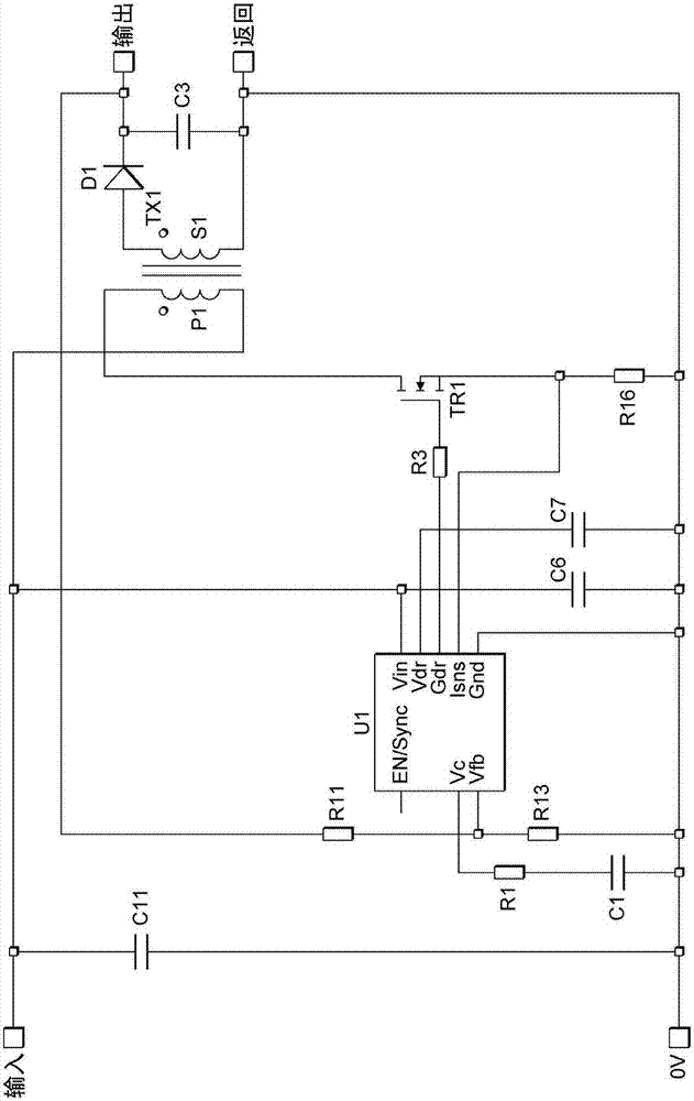
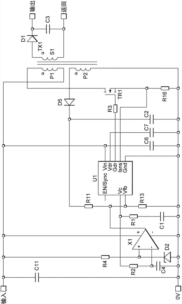
[0038] will now refer to the attached figure 2 A first embodiment of the present invention is described.
[0039] figure 2 The circuit in shows a primary-side regulated flyback power supply circuit including an auxiliary primary-side transformer winding P2. As described above, the switch circuit SC1 is implemented using the switch MOSFET TR1 and the PWM controller U1. The drain terminal of MOSFET TR1 is connected to one side of the primary transformer winding P1 while the source of MOSFET TR1 is connected to the 0V voltage rail. The operation of the switch MOSFET TR1 is controlled by a signal output from a PWM controller as known in the art. Specifically, the gate drive terminal GCR of the PWM controller U1 is connected to the gate of the switch MOSFET TR1, so that the MOSFET TR1 can be turned on and off as required to control the energy supply of the primary coil P1. The ground terminal of the PWM controller U1 is connected to the low voltage rail (0V). Otherwise assume ...
Embodiment 2
[0069] will now refer to Figure 4 A second embodiment of the present invention is described. The components and operation of the circuit are the same as those of the first embodiment. However, in Figure 4 In , the comparator X1 and reference diode D2 and resistor R4 are replaced by an adjustable precision shunt regulator U2. The shunt regulator has an internal 2.5V reference connected to its comparator non-inverting input terminal.
[0070] The cathode of the shunt regulator is connected to the auxiliary winding P2 via a diode D5 and a resistor R6. The inverting pin (ref pin) of the shunt regulator U2 is connected to the error amplifier output terminal Vc of U1 through a resistor R12. As mentioned above, the inverting pin is connected to the midpoint between the resistor R12 and the capacitor C14, and the capacitor C4 is connected to 0V.
[0071] The output of the internal comparator (its cathode pin) is not directly connected to U1's voltage feedback pin, Vfb, because ...
PUM
 Abstract
Description
Claims
Application Information


