Circuit board machining method and circuit board
A processing method and circuit board technology, which is applied in the direction of printed circuit, printed circuit manufacturing, printed circuit components, etc., can solve the problems of unfavorable PCB surface to run fine lines, occupy PCB surface wiring space, increase manufacturing cost, etc., and achieve great convenience Effect of current loading, superior conductivity, and strong current-carrying capacity
- Summary
- Abstract
- Description
- Claims
- Application Information
AI Technical Summary
Problems solved by technology
Method used
Image

Examples
Embodiment 1
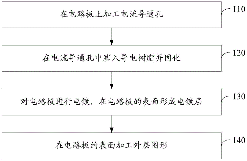
[0023] Please refer to figure 1 , an embodiment of the present invention provides a method for processing a circuit board, which may include:
[0024] 110. Processing current conduction holes on the circuit board.
[0025] The circuit board mentioned in the embodiment of the present invention may be a circuit board of any structure manufactured by any prior art. Preferably, the circuit board is a circuit board for power supply products, which has at least one thick copper circuit layer for carrying large current. The thickness of said thick copper circuit layer can be more than 10 ounces (OZ, 1OZ equals approximately 35 microns), and can be used to carry a current greater than or equal to 5A. A variety of metallized through holes generally need to be designed on the circuit board to realize interlayer transmission of current or signals. Various metallized vias include: current vias used to transfer current between layers, and signal vias used to transfer signals between lay...
Embodiment 2
[0040] Please refer to image 3 , the embodiment of the present invention also provides another circuit board processing method, which may include:
[0041] 310. Processing current conduction holes on the circuit board.
[0042]The circuit board mentioned in the embodiment of the present invention may be a circuit board of any structure manufactured by any prior art. Preferably, the circuit board is a circuit board for power supply products, which has at least one thick copper circuit layer for carrying large current. The thickness of the thick copper circuit layer can be more than 10 ounces (OZ, 1OZ is approximately equal to 35 microns), and can be used to carry a current greater than or equal to 5A. A variety of metallized through holes generally need to be designed on the circuit board to realize interlayer transmission of current or signals. Various metallized vias include: current vias used to transfer current between layers, and signal vias used to transfer signals be...
Embodiment 3
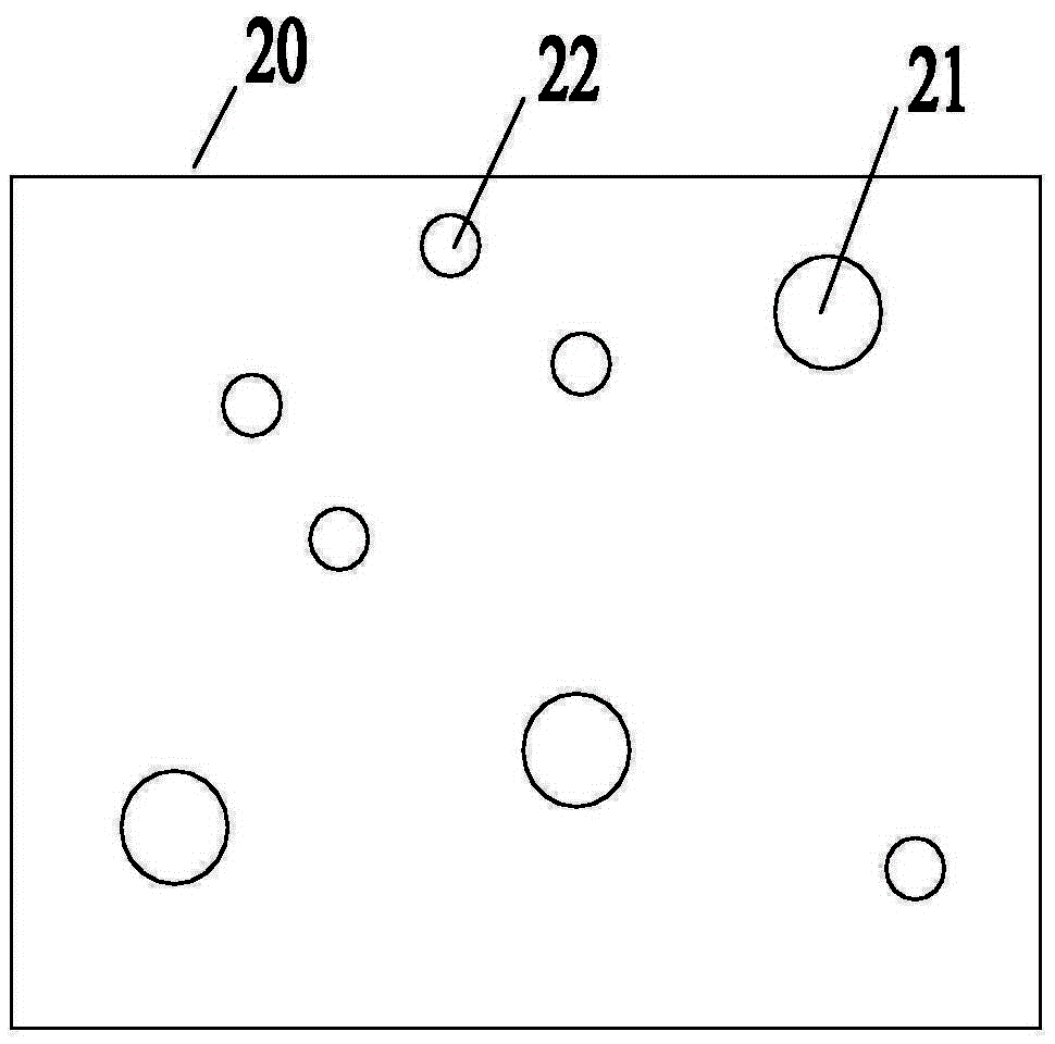
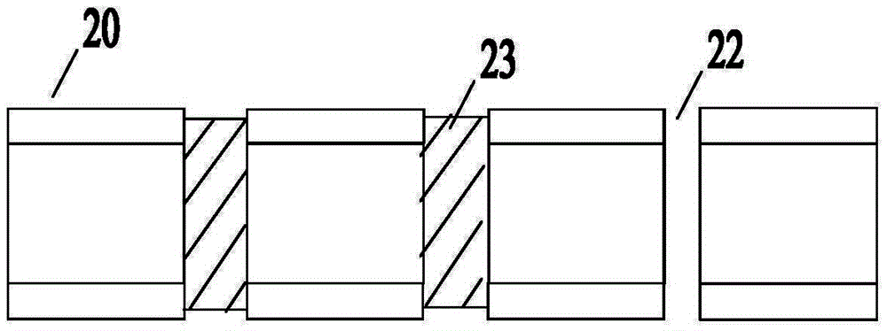
[0055] Please refer to Figure 2a-2d , the embodiment of the present invention provides a circuit board 20 .
[0056] The circuit board 20 has a current conduction hole 21 , and a conductive resin 23 is cured in the current conduction hole 21 .
[0057] The circuit board provided in this embodiment can be manufactured by the method disclosed in the first embodiment above. For a more detailed description of the circuit board 20 , please refer to the content recorded in the first embodiment.
[0058] It can be seen from the above that the embodiment of the present invention discloses a circuit board. The circuit board achieves the following technical effects by inserting conductive resin into the current conduction hole:
[0059] First, because the conductive resin or metal post is inserted into the current conduction hole, the current conduction cross section is increased, so the current conduction hole can carry a larger current, thus, the circuit board no longer needs dense ...
PUM
 Abstract
Description
Claims
Application Information