Low area full adder with shared transistors

A transistor and full adder technology, applied in the field of full adders, can solve problems such as power reduction of full adders

Active Publication Date: 2016-04-06
TEXAS INSTR INC
View PDF17 Cites 4 Cited by
  • Summary
  • Abstract
  • Description
  • Claims
  • Application Information

AI Technical Summary

Problems solved by technology

So it is obvious that as the total number of transistors decreases, the power consumed by the full adder also decreases

Method used


Image

  • Low area full adder with shared transistors
  • Low area full adder with shared transistors
  • Low area full adder with shared transistors

Examples


Embodiment Construction

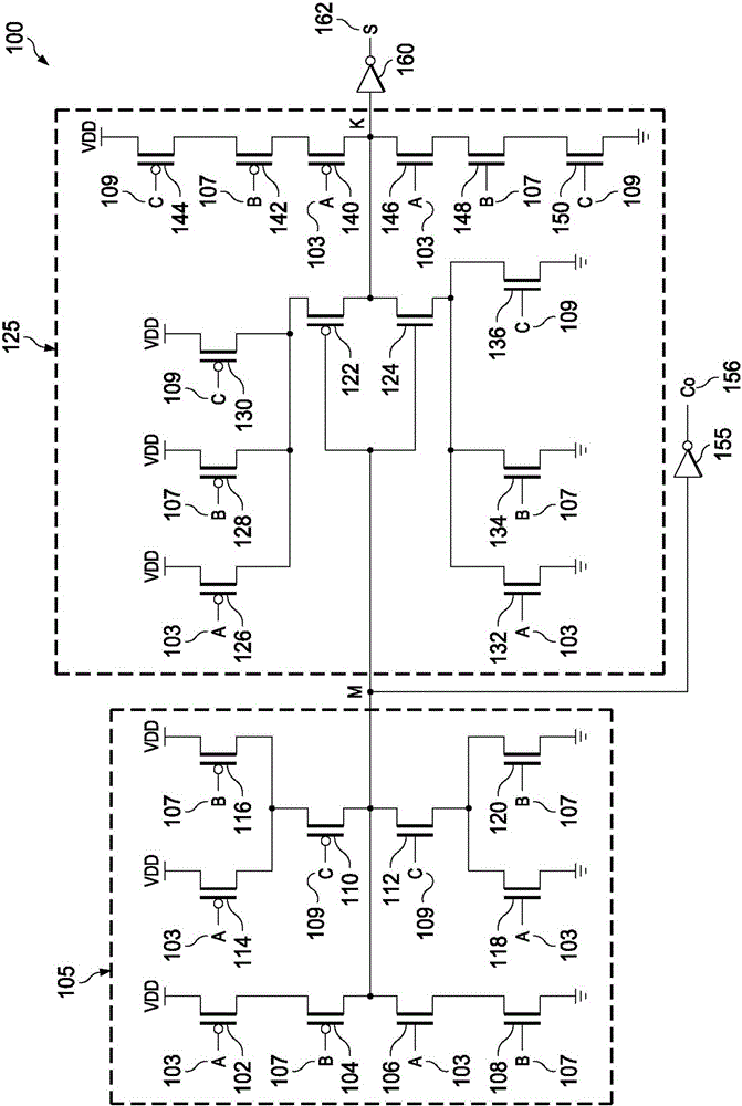
[0012] FIG. 1 shows a conventional full adder 100 . The conventional full adder 100 includes a carry generating circuit 105 , a sum generating circuit 125 , a first inverter 155 and a second inverter 160 . The carry generating circuit 105 is now explained. The carry generating circuit 105 comprises a first PMOS transistor 102 having a gate terminal receiving a first input A103 and a source terminal being coupled to a power supply terminal VDD. The drain terminal of the first PMOS transistor 102 is coupled to the source terminal of the second PMOS transistor 104 . The gate terminal of the second PMOS transistor 104 receives a second input B107.

[0013] The drain terminal of the second PMOS transistor 104 is coupled to the first node M. As shown in FIG. The carry generating circuit 105 further comprises a first NMOS transistor 106 having a gate terminal receiving the first input A103 and a drain terminal being coupled to the first node M . The source terminal of the first N...


PUM


Abstract

The invention relates to a low area full adder with shared transistors. A full adder (200) is disclosed that utilizes low area. The full adder (200) includes an exclusive NOR logic circuit (205). The exclusive NOR logic circuit (205) receives a first input (202) and a second input (204). A first inverter (235) receives an output (234) of the exclusive NOR logic circuit (205) and generates an exclusive OR output (236). A carry generation circuit (245) receives the output (234) of the exclusive NOR logic circuit (205), the exclusive OR output (236) and a third input (206). The carry generation circuit (245) generates an inverted carry (246). A second inverter (247) is coupled to the carry generation circuit (245) and generates a carry (248) on receiving the inverted carry (246). A sum generation circuit (250) receives the output (234) of the exclusive NOR logic circuit (205), the exclusive OR output (236) and the third input (206). The sum generation circuit (250) generates an inverted sum. A third inverter (265) is coupled to the sum generation circuit (250) and generates a sum (270) on receiving the inverted sum.

Description

technical field [0001] The present invention relates to an integrated circuit, and more particularly to a full adder implemented using MOS transistors. Background technique [0002] Due to the continued development of integrated circuits (ICs), full adders occupy the majority of the area and power of any circuit design. The units in the IC that consume power are logic implementations, full adders, flip-flops, RAM, clock trees, and integrated clock gating (ICG) units. A full adder consumes 30-40% of the total area and 30-40% of the total power in a typical digital design. [0003] The power consumed by a full adder is proportional to the number of transistors used to implement the full adder. Therefore, it is obvious that as the total number of transistors decreases, the power consumed by the full adder also decreases. Likewise, a reduction in the area of ​​the full adder translates directly into a reduction in chip area and cost savings. Also, since full adders are the m...

Claims


Application Information

Patent Timeline
Patent Type & Authority Applications(China)
IPC IPC(8): H03K19/20
CPCG06F7/501H03K19/20H03K19/0013G06F7/50
Inventor S·南迪B·M·苏班纳瓦
Owner TEXAS INSTR INC
Why Eureka
Try Eureka