Multi-function differential logic gate

a multi-functional, differential logic technology, applied in logic circuits, oscillation comparator circuits, pulse techniques, etc., can solve problems such as inability to take advantage of differential signaling benefits

Inactive Publication Date: 2005-11-03
SEIKO EPSON CORP
View PDF14 Cites 2 Cited by
  • Summary
  • Abstract
  • Description
  • Claims
  • Application Information

AI Technical Summary

Benefits of technology

[0008] It is a further object of the present invention to provide multi-function differential logic gate that can be made to selectively behave as a differential AND gate or differential OR gate without altering its architecture or using a specific behavior altering control input.

Problems solved by technology

It is well known that differential CMOS circuits, especially current mode logic circuits (CML), are generally faster and generate lower noise than single-ended CMOS circuits, but since PFD circuits are single-ended circuits they cannot take advantage of the benefits of differential signaling.

Method used


Image

  • Multi-function differential logic gate
  • Multi-function differential logic gate
  • Multi-function differential logic gate

Examples


Embodiment Construction

[0022] Preferred embodiments of the present invention are described below with reference to the accompanying figures.

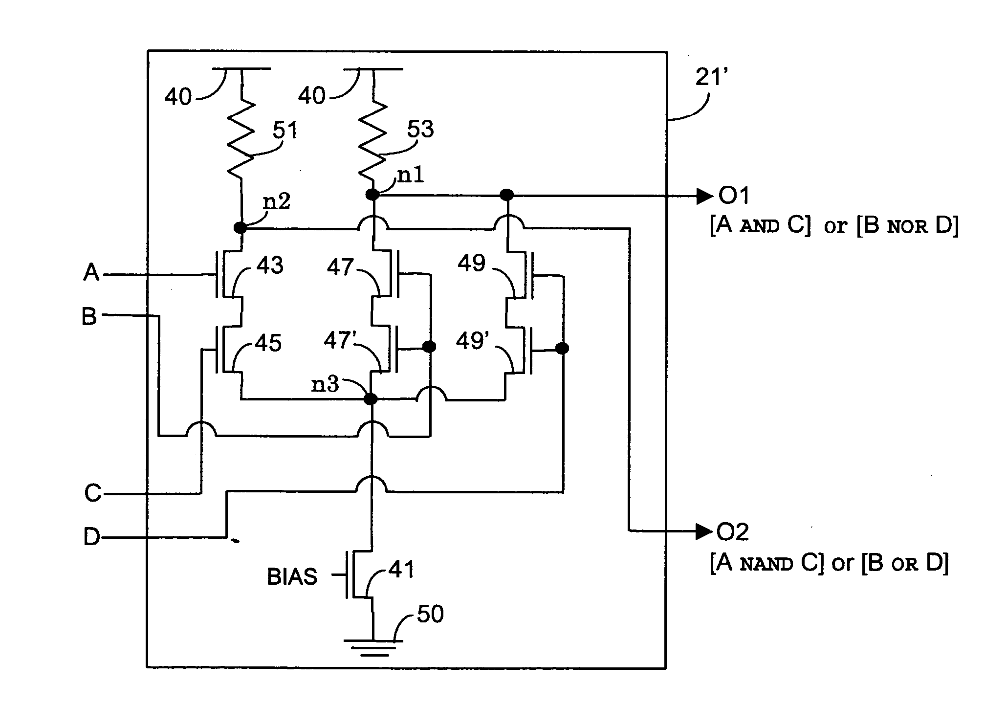
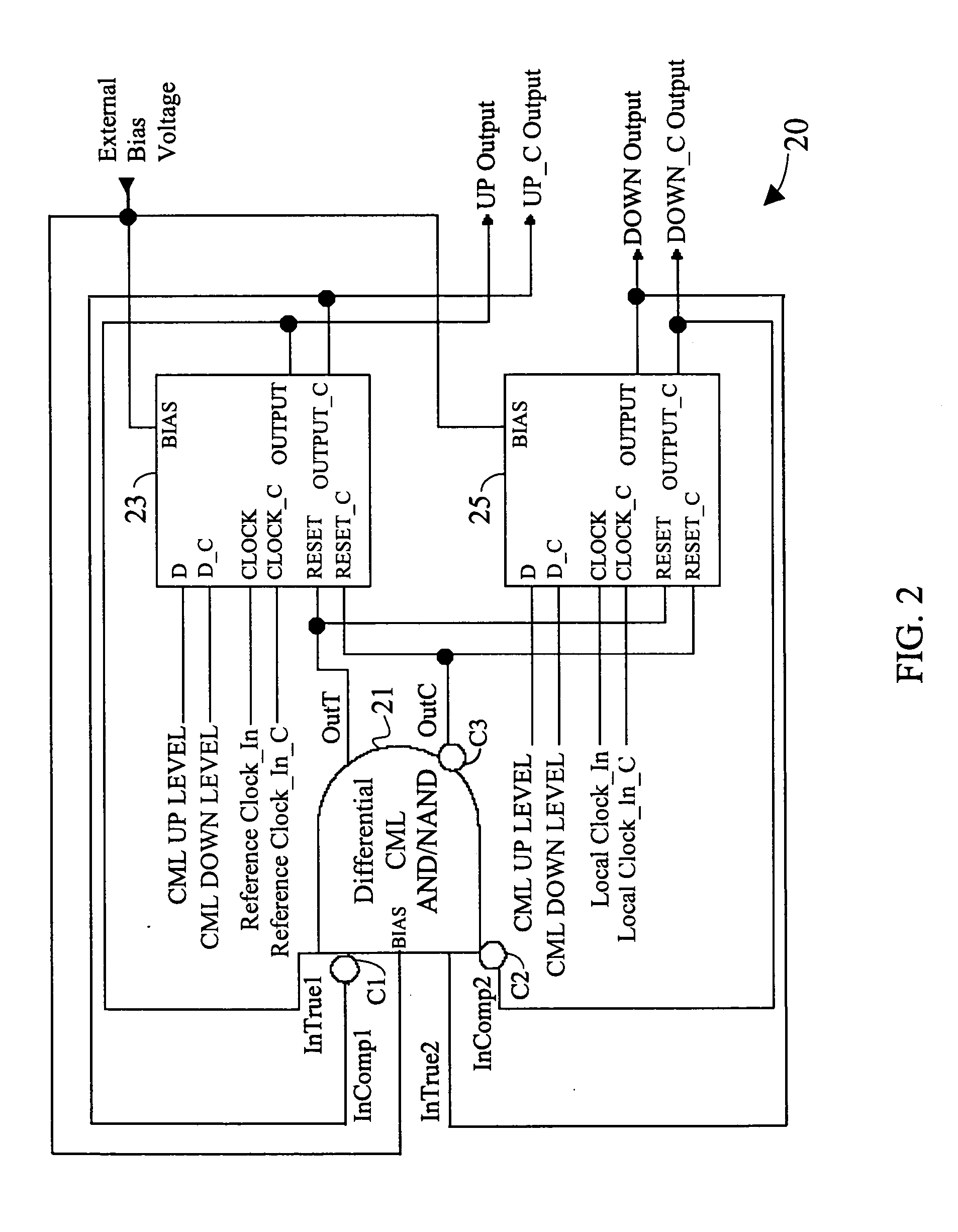
[0023] With reference to FIG. 2, a fully differential phase and frequency detector, PFD, 20 in accord with the present invention utilizes a fully differential AND gate 21, and two fully differential D-flip-flops 23 and 25. In the present embodiment, a fully differential reference clock (i.e. true signal Reference Clock_In and complement signal Reference Clock_In_C) is compared with a fully differential local clock (i.e. true signal Local Clock_In and complement signal Local Clock_In_C). D-flip-flops 23 and 25 also have fully differential UP / UP_C and DOWN / DOWN_C outputs, which are coupled to drive a fully differential charge pump. Such a charge pump is well know, and disclosed, for example, in IEEE JSSC 35:6 p 852, which is hereby incorporated in its entirety by reference. Preferably, the differential PFD 20 is implemented in current mode logic, CML, as explained in m...


PUM


Abstract

A fully differential phase and frequency detector utilizes a multi-function differential logic gate to implement a differential AND gate operation and provides a fully differential D-flip-flop. The multi-function differential logic gate has four inputs, which can be grouped into two pairs of true and complement signals. By selectively re-assigning the inputs to different signal pairs, the differential logic gate can be made to provide one of either simultaneous AND/NAND logic operations or simultaneous OR/NOR logic operations. The differential D-flip-flop is implemented following a master/slave configuration and is response to the true and complement forms of an input clock signal, an input reset input, and input data signal, and also provides true and complement forms of an output signal. All components within the phase and frequency detector are exemplified in CML circuit configuration.

Description

BACKGROUND OF THE INVENTION [0001] 1. Field of the Invention [0002] The present invention relates generally to differential logic gates, such as can be used in CMOS phase and frequency detector (PFD) circuits used in the locking of phase locked loops (PLL) and delay locked loops (DLL). This invention relates more specifically to a differential AND gate, a differential OR gate and a multi-function differential AND / OR gate. [0003] 2. Description of the Related Art [0004] High speed phase locked loops (PLL) are used in modern communication systems for many purposes, including clock generation and data recovery and retiming. Typically, the input signal for the reference input of a PLL is a differential signal where the crossing of the true and complement signals represents the clock transition. However, phase and frequency detector circuits (PFD) used for clock multiplication and generation are typically single-ended circuits. When a differential reference signal is provided to a PFD, e...

Claims


Application Information

Patent Timeline
Patent Type & Authority Applications(United States)
IPC IPC(8): H03K3/3562H03D13/00H03K3/356H03K19/094H03K19/096H03K19/20H03L7/085H03L7/089
CPCH03D13/00H03L7/085H03K3/356043
Inventor MELTZER, DAVIDPADAPARAMBIL, MURALIKUMAR A.WU, TAT C.
Owner SEIKO EPSON CORP
Why Eureka
Try Eureka