
Laser engraving manufacturing process for fine circuit

A manufacturing process and fine circuit technology, applied in the direction of printed circuit manufacturing, printed circuit, electrical components, etc., can solve the problems of abnormal mass production, disconnection and overflow plating, and large labor costs, so as to meet the needs of mass production and avoid Disconnection and high work efficiency

Inactive Publication Date: 2016-04-06
东莞光韵达光电科技有限公司
View PDF4 Cites 7 Cited by
  • Summary
  • Abstract
  • Description
  • Claims
  • Application Information

AI Technical Summary

Problems solved by technology

[0003] However, at present, the fine lines of 0.1mm and below will face the problems of disconnection and overflow plating during production, which cannot be mass-produced normally, or the produced products need to spend a lot of manual post-processing, which is very expensive

Method used


Image

  • Laser engraving manufacturing process for fine circuit
  • Laser engraving manufacturing process for fine circuit
  • Laser engraving manufacturing process for fine circuit

Examples


Embodiment Construction

[0015] The present invention will be further elaborated below in conjunction with accompanying drawing:

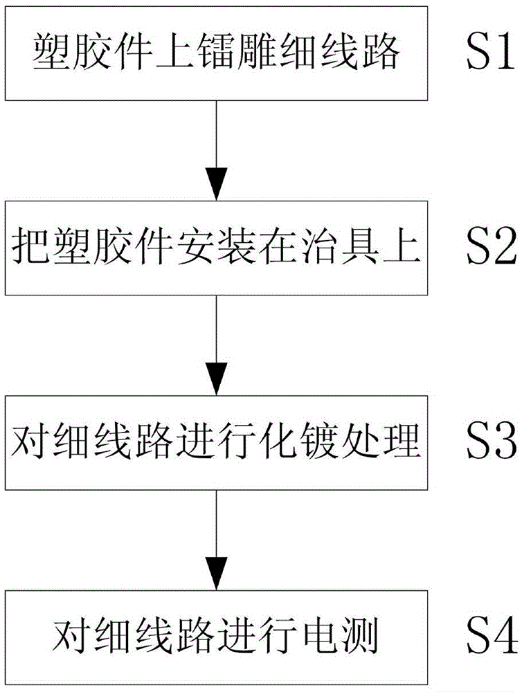
[0016] The invention provides a fine line radium engraving manufacturing process, such as figure 1 As shown, the manufacturing process includes the following steps:

[0017] Step 1, use the LDS laser machine to carve thin lines with a width of ≤0.1mm on the LDS plastic parts;

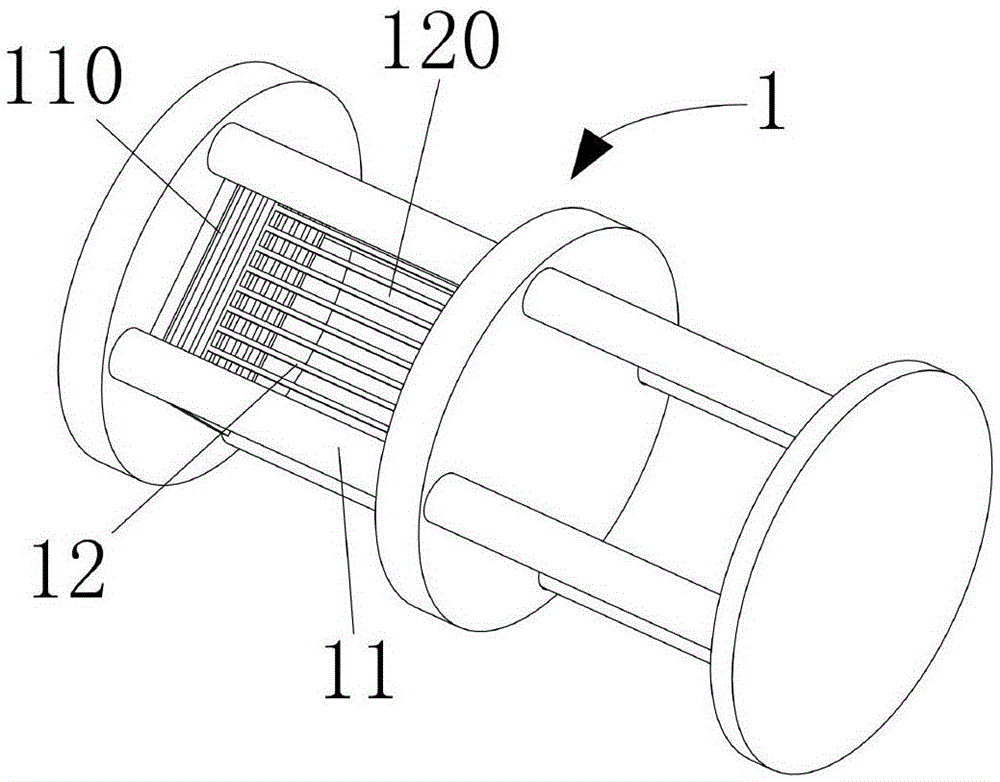
[0018] Step 2, install the laser-carved plastic parts on the jig combining the roller and the hanger;

[0019] Step 3, with the movement of the jig, perform electroless plating on the plastic parts carved with radium, and obtain the required metal layer on the line;

[0020] Step 4, conduct an electrical test on the circuit after obtaining the metal layer.

[0021] In the above process, the parameters of the LDS laser machine include: laser power: 1-20W; laser scanning speed: 1000-4000mm / s; laser frequency: 20-200KHZ. The laser machine uses the light energy of the laser beam to cause the chemica...


PUM


Abstract

The invention relates to a laser engraving manufacturing process for a fine circuit. The manufacturing process comprises the following steps: step 1, preparing a thin circuit with a width of less than or equal to 0.1 mm through a laser engraving manner in an LDS plastic part by utilizing an LDS laser; step 2, mounting the laser engraved plastic part on a jig that combines a roller and a suspension frame; step 3, performing chemical plating treatment on the laser engraved plastic part to obtain a required metal layer on the circuit; and step 4, performing electrical logging on the circuit after the metal layer is obtained. By adoption of the laser engraving manufacturing process for the fine circuit, large-scale production of the fine circuit with the thickness of less than or equal to 0.1 mm can be realized, and the applied range of the LDS process is expanded.

Description

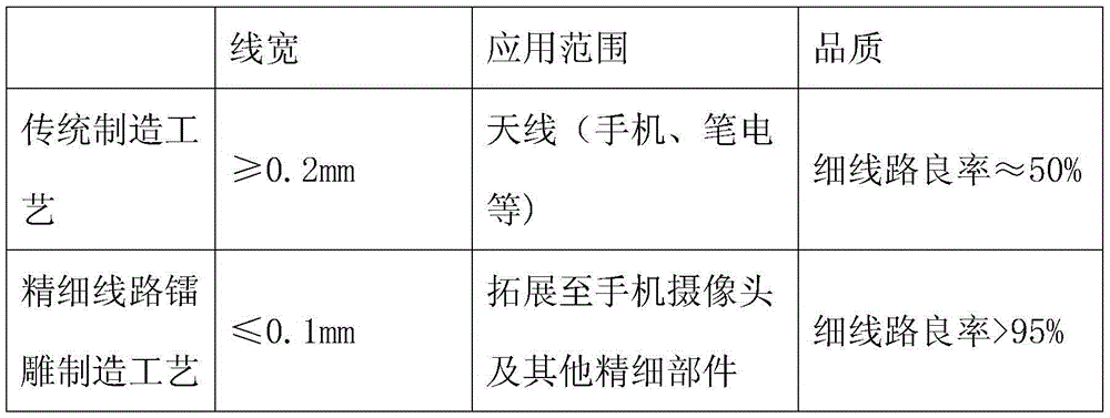
technical field [0001] The invention relates to a fine circuit radium engraving manufacturing process. Background technique [0002] In the field of LDS manufacturing, the usual line width and line spacing requirements are mostly above 0.2mm, which can basically meet the requirements of ordinary antennas and connectors. However, for the requirements of fine components and special products, the line width and line spacing need to be further reduced to 0.1mm or less. [0003] However, at present, the fine lines of 0.1mm and below will face the problems of disconnection and overflow plating during production, which cannot be mass-produced normally, or the produced products require a lot of manual post-processing, which is very costly. Contents of the invention [0004] In order to solve the above problems, the present invention provides a fine circuit radium engraving manufacturing process, which is characterized in that the manufacturing process includes the following steps...

Claims


Application Information

Patent Timeline
Patent Type & Authority Applications(China)
IPC IPC(8): H05K3/18
CPCH05K3/18H05K2203/107
Inventor 姚彩虹王革杰
Owner 东莞光韵达光电科技有限公司
Learn More