Realization method for film preparation by applying atomic layer deposition technology

A technology of atomic layer deposition and realization method, applied in coating, metal material coating process, gaseous chemical plating, etc., can solve the problem of purging the precursors and reaction by-products that are not easy to clean, increase the purging time and inert gas Consumption, reducing ALD yield and other issues, to achieve the effect of reducing parasitic CVD reaction, improving ALD process quality, and improving purging effect

Active Publication Date: 2016-04-20
BEIJING NAURA MICROELECTRONICS EQUIP CO LTD
View PDF10 Cites 11 Cited by
  • Summary
  • Abstract
  • Description
  • Claims
  • Application Information

AI Technical Summary

Problems solved by technology

[0006] However, the above-mentioned conventional ALD technology also has some disadvantages: firstly, the use of the above-mentioned purging method will make the gas flow field in the reaction chamber relatively stable, resulting in the existence of dead zones in the chamber space, so that it is not easy to remove excess precursors and reactants. The by-products are purged clean; secondly, the use of the above-mentioned purging method will increase the purging time and the consumption of inert gas, thereby reducing the yield of ALD

Method used


Image

  • Realization method for film preparation by applying atomic layer deposition technology
  • Realization method for film preparation by applying atomic layer deposition technology
  • Realization method for film preparation by applying atomic layer deposition technology

Examples


Embodiment 1

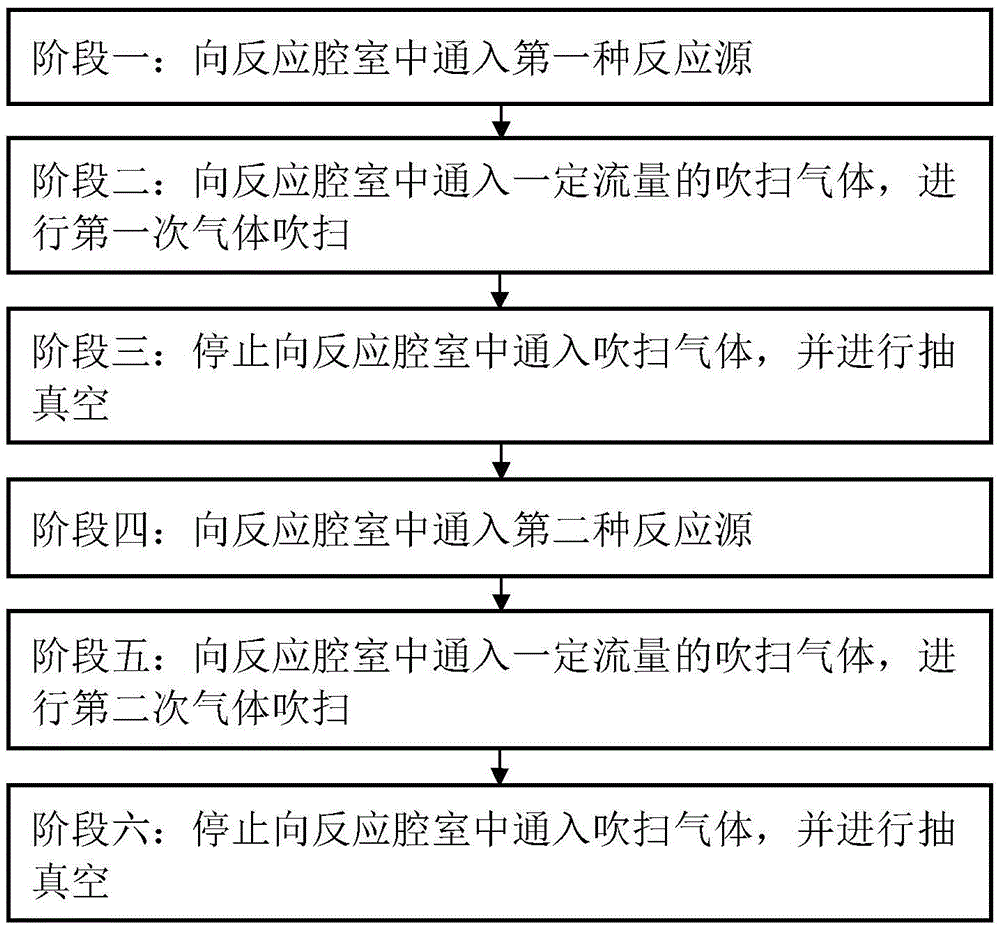
[0081] The vacuum-type ALD process is used for 200 cycles of film growth to prepare an aluminum oxide film with a target thickness of 20nm. The ALD process parameters are: process temperature 200°C, ALD process cycle (passing TMA for 2s, vacuuming for 2s, purging for 2s, and passing O 3 2s, vacuuming 2s, purging 2s) a total of 12s. Please refer to Figure 4 block diagram.

[0082] The result of the process is that the obtained film has a thickness of 20.5 nm and an intra-chip uniformity of 2%.

Embodiment 2

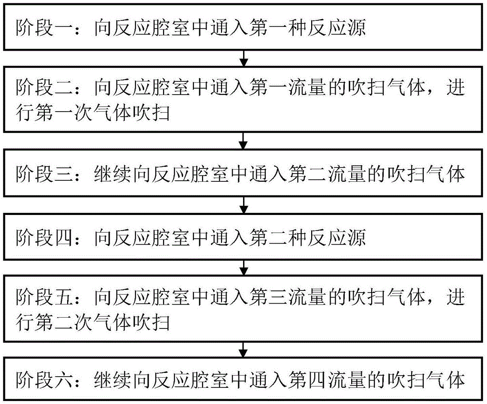
[0084] 200 cycles of film growth were performed using a vacuum-type ALD process to prepare an aluminum oxide film with a target thickness of 20nm. 3 2s, purge 2s, vacuum 2s) total 12s. Please refer to Figure 5 block diagram.

[0085] The result of the process is that the obtained film has a thickness of 21.5 nm and an intra-chip uniformity of 1.5%.

Embodiment 3

[0087] 200 cycles of film growth were performed using a vacuum-type ALD process to prepare an aluminum oxide film with a target thickness of 20nm. 3 2s, vacuuming 2s, purging 2s) a total of 12s. Please refer to Figure 6 block diagram.

[0088] The result of the process is that the obtained film has a thickness of 22.5 nm and an intra-chip uniformity of 2.5%.


PUM

PropertyMeasurementUnit
thicknessaaaaaaaaaa
thicknessaaaaaaaaaa
thicknessaaaaaaaaaa

Abstract

The invention discloses a realization method for film preparation by applying an atomic layer deposition technology. A different ALD technological mode of a vacuumizing mode or a variable flow mode is used for changing an intake quantity of sweeping gas in a reaction cavity to form disturbance of an airflow field in the cavity, so that the sweeping effect on a surplus reaction source and a reaction byproduct can be effectively improved, the process time of film growth period is shortened, the productivity is improved, the parasitic CVD reaction can be reduced on the basis, the ALD process quality is improved, and the film uniformity is improved.

Description

technical field [0001] The invention relates to the technical field of atomic layer deposition, and more specifically, to a method for preparing a thin film by applying the atomic layer deposition technology. Background technique [0002] Atomic layer deposition (Atomic layer deposition, ALD) is a method (technology) of forming a deposited film by alternately passing gas-phase precursors into the reactor and chemically reacting on the surface of the substrate. The form is plated on the surface of the substrate layer by layer. [0003] During the atomic layer deposition process, when the precursor reaches the surface of the deposition substrate, it will be deposited on the surface of the substrate in the form of chemical adsorption. The reactor needs to be purged with an inert gas between different precursor pulses to remove excess reaction sources that are not adsorbed on the surface of the substrate and ensure that chemical reactions only occur on the surface of the substr...

Claims


Application Information

Patent Timeline
Patent Type & Authority Applications(China)
IPC IPC(8): C23C16/455
CPCC23C16/45525
Inventor 李春雷赵雷超胡彩丰
Owner BEIJING NAURA MICROELECTRONICS EQUIP CO LTD
Why Eureka
Try Eureka